In the following Python script it is shown how the aliasing effect (having signals whose frequency is beyond half of the sampling frequency, i.e., \(\frac{f_s}{2}\)) can be intuitively understood as a folding of the frequencies outside the \(\left[0, \frac{f_s}{2}\right]\) range.

In the script, the sampling frequency is 10 kHz. Then, 3 sinusoids of frequency \(f_{s1} = 500~Hz\), \(f_{s2} = 6~kHz\) and \(f_{s3} = 11~kHz\) are generated. The FFT of the sum of s1, s2 and s3 is computed and plotted. Given that the Nyquist frequency in the system is 5 kHz, it can be seen on the FFT plot how the frequencies wrap around \(\frac{f_s}{2}\) and 0.

Just as a reminder, the way the X-axis on the FFT is explained in FFT resolution.

import numpy as np
import numpy.fft as fft
import matplotlib.pyplot as plt

# Define sampling frequency 
fs = 10e3
Ts = 1/fs

# Define time array
n_periods = 1000
total_time = 1/fs * n_periods
t = np.arange(0, total_time, Ts)


# %% Define signal 1
f1 = 500
s1 = np.sin(2*np.pi*f1*t)


# %% Define signal 2
# Since fs = 5_000, f2 will fold to 4_000 Hz bin
f2 = 6_000
s2 = 0.5 * np.sin(2*np.pi*f2*t)

# %% Define signal 3
# Since fs = 5_000, f3 will fold first on 5_000 Hz and then on 0 again. Therefore, f3 will be shown at 1_000 Hz bin
f3 = 11_000
s3 = 0.25 * np.sin(2*np.pi*f3*t)

# %% Define signal as a sum of s1, s2 and s3
s = s1 + s2 + s3

# %% Compute FFT 
# Total number of samples 
N_samples = len(s)
print(f"Number of samples: {N_samples}")
# Floor in case division is not integer
half_N_samples = int(np.floor(N_samples/2))
# Define frequency bin width 
delta_f = fs/N_samples

# Compute frequency bins until Nyquist frequency
freq_bins = np.arange(0, fs/2, delta_f)

Y = fft.fft(s)

plt.figure(figsize=(8,6), dpi=300)

# Plot only half of the FFT result. Plot absolute value and scale it to represent amplitude
plt.plot(freq_bins, 2.0 / N_samples * np.abs(Y)[:half_N_samples])
plt.grid(True, which='both')
plt.minorticks_on()
plt.title('Signal FFT')
plt.xlabel('Frequency (Hz)')
plt.ylabel('Amplitude')
plt.show()

Motivation

Several months ago I started trying to find how charge distribution across different capacitors works and I came up to this thought experiment. I used CircuitLab to simulate it and confirm what my intuition said it would ocurr. However, this intuition was wrong and led me to post this question in Electronical Engineering of Stack Exchange in order to find an explanation. Several people took some time to answer the question (really appreaciated), however the answers were not actually satisfactory since they were not really explaining analytically what was behind it. Arout seven months later, I finally found the solution thanks to this video.

For a basic explanation on how to deal with capacitors and charge, please refer to this previous post, written the very same day I started struggling trying to find a solution to this.

Explanation

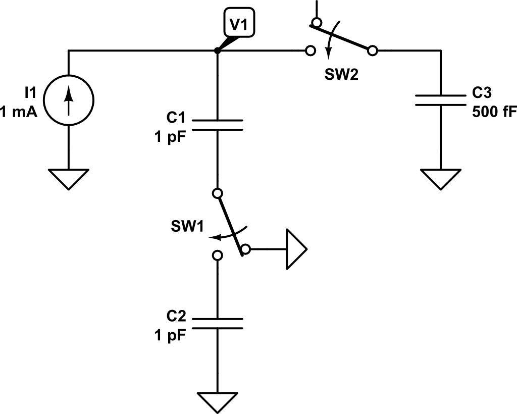
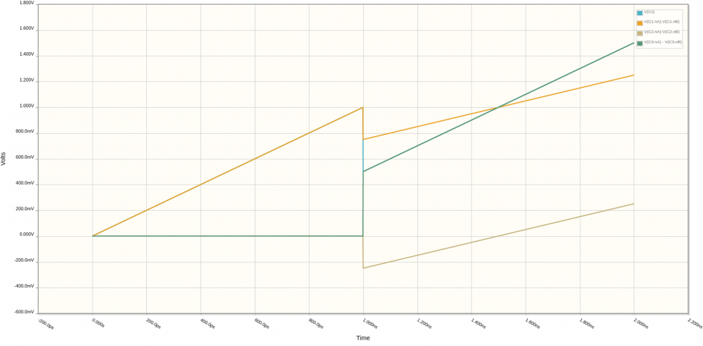
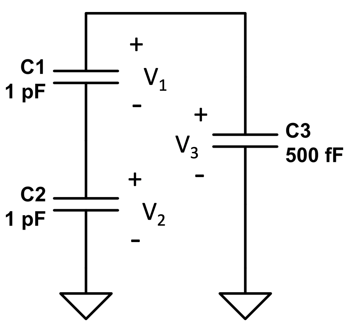
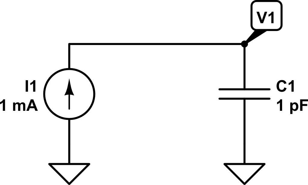
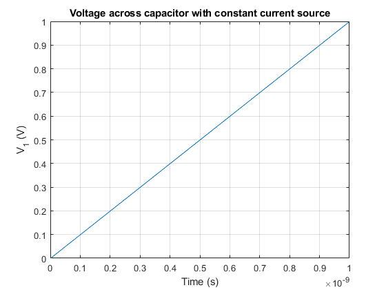
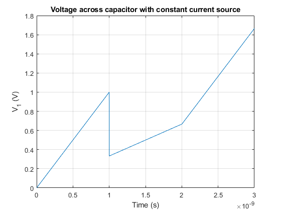
In this circuit, there is an independent DC current source of \(1~mA\) and switches SW1 and SW2 are closed at time \(t=t_1 = 1ns\). From time \(0 < t < t_1\), only \(C_1\) is connected to the current source, so the expected voltage \(V_1\) could be expressed as:

\[V_1 \left( t \right) = \int{\frac{i_1}{C_1}dt} = \frac{i_1 \cdot t}{C_1}\]

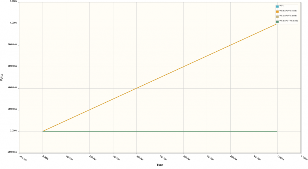
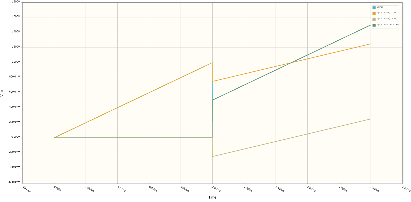
The rest of capacitors are discharged and therefore its voltage is \(0~V\) as shown in the following plot:

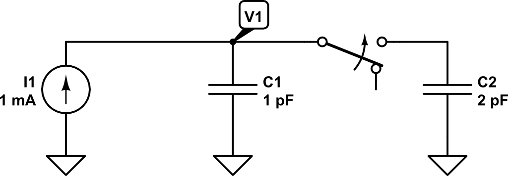
Now, at time \(t = t_1 = 1 ns\), switches SW1 and SW2 are closed and capacitors \(C_2\) and \(C_3\) are connected to the circuit. At this point, the current source will keep injecting charge into the capacitors. However, we need first to compute how charge is distributed across capacitors \(C_1\), \(C_2\), \(C_3\). The total charge of the circuit at time \(t = t^-_1\) is:

\[Q_T\left(t^-_1\right) = Q_1 = C_1 \cdot V_1\left(t_1\right)\]

\[V_1\left(t_1\right) = \frac{i_1 \cdot t_1}{C_1} = \frac{1~mA\cdot 1ns}{1~pF} = 1~V\]

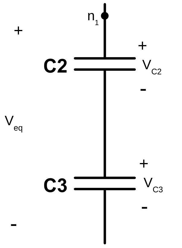
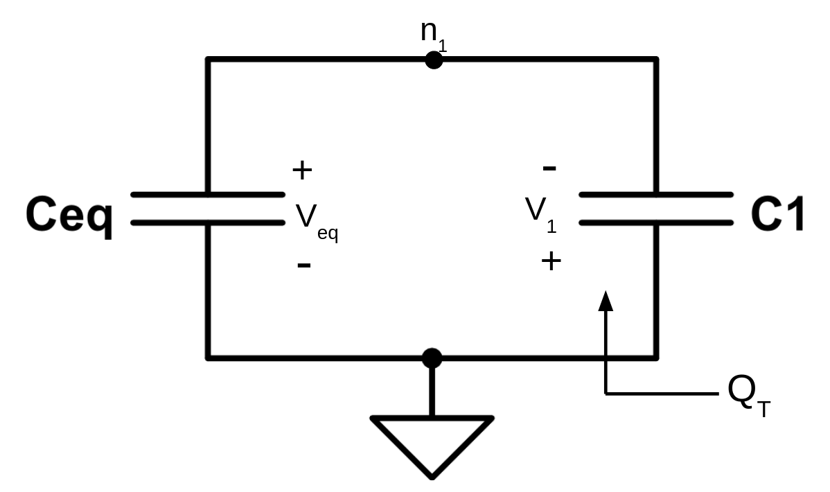
By applying superposition theorem, we can determine the contribution of the \(C_1\) voltage on the rest of capacitors. To do so, let’s analyze the following equivalent circuit:

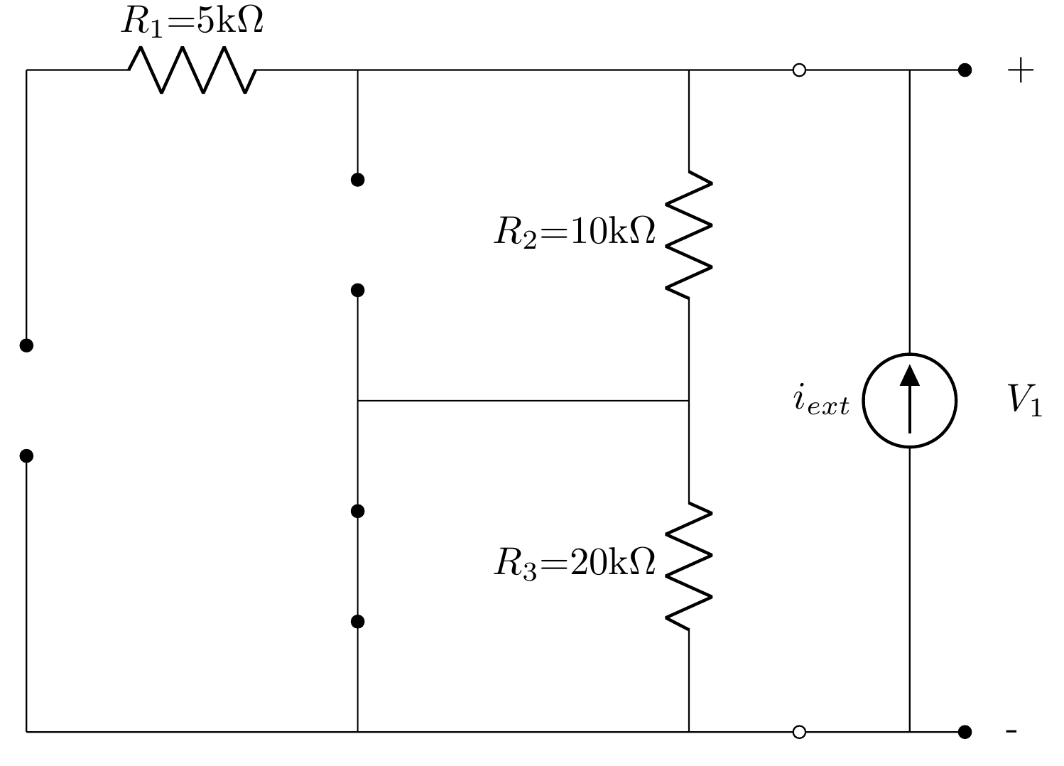
Capacitors \(C_2\) and \(C_3\) are actually connected in series since they share the ground node. So, the circuit could be arranged in the following manner:


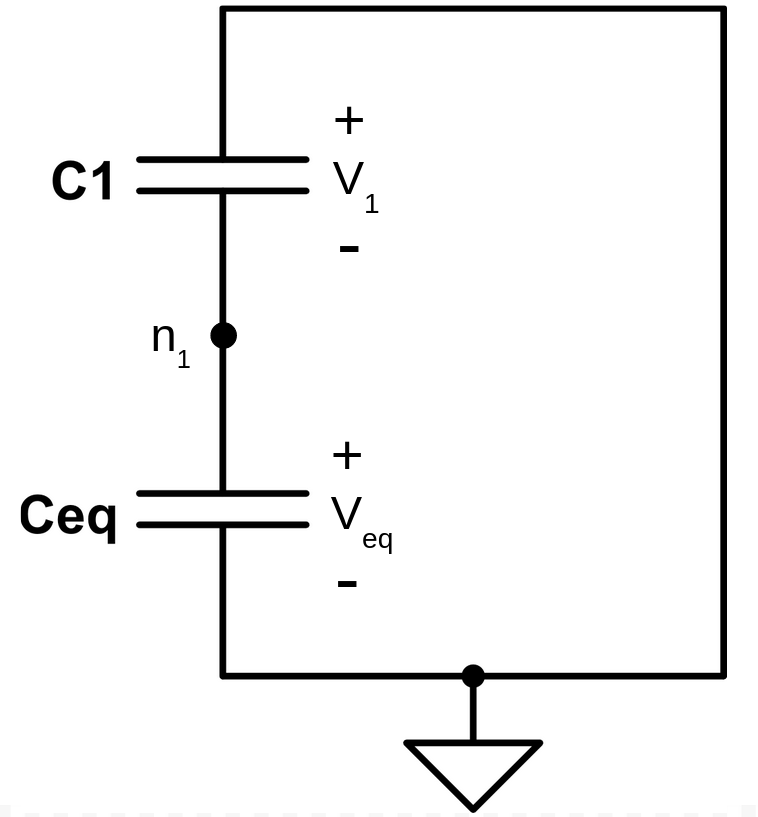
The equivalent capacitance would be:

\[ C_{eq} = \frac{C_2 \cdot C_3}{C_2 + C_3} \]

Now, let’s compute the total charge of the system. To do so, let’s rearrange again the circuit. In order to be able to compare the total charge at \(t = t^+_1\) with the total charge \(Q_T\left(t^-_1\right)\), we need to keep being compliant with sign declaration. So \(Q_T\) must be computed from the following point:

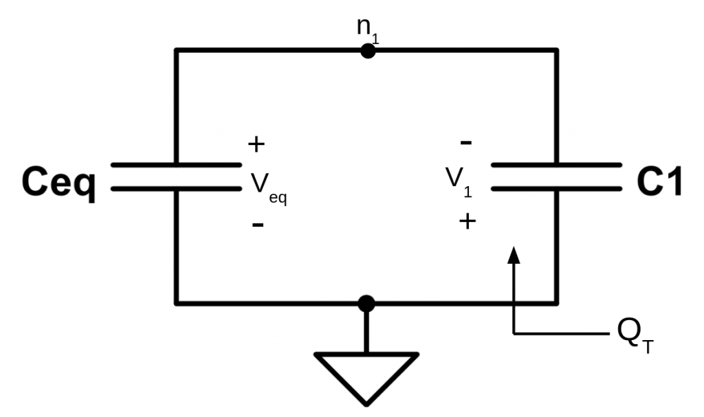
Then, the total charge of the system \(Q_T\left(t^+_1\right)\) would be:

\[Q_T\left(t^+_1\right)= Q_1 – Q_{eq} = V_1\left(t^+_1\right) \cdot C_1 – V_{eq}\left(t^+_1\right) \cdot C_{eq}\]

Due to the way the capacitors are connected, we can assert that \(V_{eq} = -V_1\). Therefore, the total charge of the system can be expressed as a function of \(V_1\):

\[Q_T\left(t^+_1\right)= V_1\left(t^+_1\right) \cdot C_1 – V_{eq}\left(t^+_1\right) \cdot C_{eq} = V_{1}\left(t^+_1\right) \cdot C_{1} + V_1\left(t^+_1\right) \cdot C_{eq}\]

Since the charge in the system must keep constant after the switches position changed, it can be said that:

\[ Q_T\left(t^-_1\right) = Q_T\left(t^+_1\right)\]

This can be expanded to:

\[ C_1 \cdot V_1\left(t^-_1\right) = V_{1}\left(t^+_1\right) \cdot C_{1} + V_1\left(t^+_1\right) \cdot C_{eq}\]

Solving for the new \(V_1\) at time \(t = t^+_1\):

\[ V_1\left(t^+_1\right) = \frac{C_1}{C_1 + C_{eq}} V_1\left(t^-_1\right) \]

Using the values of our example, i.e. \(C_1 = 1~pF\) and \(C_{eq} = \frac{1~pF\cdot0.5~pF}{1~pF+0.5~pF} = 0.333~pF\):

\[ V_1\left(t^+_1\right) = \frac{1~pF}{1~pF + 0.333~pF} \cdot 1~V = 0.75~V \]

\[ V_{eq}\left(t^+_1\right) = -0.75~V \]

Now, we just need to compute the voltages at capacitors \(C_2\) and \(C_3\).

Since voltage \(V_{eq}\) across them is known, we can compute the voltages \(V_{C3}\) and \(V_{C2}\) by solving the capacitive divider they constitute:

\[V_{C3} = \frac{C_2}{C_2 + C_3} V_{eq}\]

\[V_{C2} = \frac{C_3}{C_2+C_3}V_{eq}\]

Replacing the previous expressions with our example values, we get the following voltages:

\[V_{C3} = \frac{1~pF}{1~pF + 0.5~pF}\cdot\left(-0.75\right) = -0.5~V \]

\[V_{C2} = \frac{0.5~pF}{1~pF + 0.5~pF}\cdot\left(-0.75\right) =  -0.25~V\]

Finally, we can conclude that:

\[ V_{2} = V_{C2} = -0.25~V\]

\[ V_{3} = -V_{C3} = 0.5~V\]

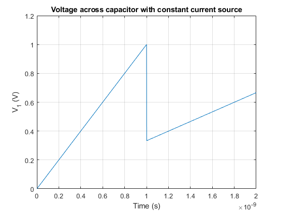
Theses results are confirmed in simulation:

A = [1, 2, 3]
B = [4, 5]
C = [6, 7, 8]
# Visit all combinations of A, B and C values
all = [A, B, C]

# General pointer. Points to the current variable: 0 -> A, 1 -> B, ...
gp = 0
# Internal pointer. Points to the item on the current variable
# Example: gp = 1 --> B selected. ip = 2 --> B[2] selected --> B[2] = 5
ip = [0] * len(all)

def iterator(a):
# For Python to get gp from global scope
global gp
# Weird way in Python to create a for loop. Equivalent in C to:
# for(int i = 0; i < len(a[0]); i++)
for i in range(0, len(a[0])):
# Store current internal pointer
ip[gp] = i
# If a has more variables (e.g. a = [[1,2,3], [4,5], [6,7,8]])
if len(a) > 1:
# Create subset for the remaining variables, i.e. [[4,5], [6,7,8]]
# Pythonic way to create an array subset from a given index until
# end of the array
b = a[1:]
# Increase global index as we are about to sweep next variables
gp = gp + 1
# Iterate the rest of variables, i.e. [[4,5], [6,7,8]]
iterator(b)
# We came back from lower variables (B and C), so restoring global
# pointer to point again to A
gp = gp - 1
else:
# Just for result visualization purposes
str = "["
# External index and internal index
for i_ext, i_in in enumerate(ip):
str = str + "{}, ".format(all[i_ext][i_in])
# Remove last ", " and add closing ] (cosmetic)
str = str.strip(", ") + "]"
print("Indexes = {} --> Values: {}".format(ip, str))

# ip contains the indexes to all internal variables. Example:
# Iterating at A[3], B[2], C[1] --> ig = [3, 2, 1]


iterator(all)

Result

Given the input variables:

A = [1, 2, 3]
B = [4, 5]
C = [6, 7, 8]

the output of the script is as follows:

Indexes = [0, 0, 0] --> Values: [1, 4, 6]
Indexes = [0, 0, 1] --> Values: [1, 4, 7]
Indexes = [0, 0, 2] --> Values: [1, 4, 8]
Indexes = [0, 1, 0] --> Values: [1, 5, 6]
Indexes = [0, 1, 1] --> Values: [1, 5, 7]
Indexes = [0, 1, 2] --> Values: [1, 5, 8]
Indexes = [1, 0, 0] --> Values: [2, 4, 6]
Indexes = [1, 0, 1] --> Values: [2, 4, 7]
Indexes = [1, 0, 2] --> Values: [2, 4, 8]
Indexes = [1, 1, 0] --> Values: [2, 5, 6]
Indexes = [1, 1, 1] --> Values: [2, 5, 7]
Indexes = [1, 1, 2] --> Values: [2, 5, 8]
Indexes = [2, 0, 0] --> Values: [3, 4, 6]
Indexes = [2, 0, 1] --> Values: [3, 4, 7]
Indexes = [2, 0, 2] --> Values: [3, 4, 8]
Indexes = [2, 1, 0] --> Values: [3, 5, 6]
Indexes = [2, 1, 1] --> Values: [3, 5, 7]
Indexes = [2, 1, 2] --> Values: [3, 5, 8]

1. Install SimpleSSHD in your mobile

2. In order to start data transfers, you can use the rsync command which has the following syntax:

rsync [-switches] ORIGIN_PATH DESTINATION_PATH

To copy from phone to computer:

rsync --update --progress -e 'ssh -p 2222' -azv 192.168.1.112:/sdcard/DCIM/Camera /computer-path

To copy from computer to phone:

rsync --update --progress -e 'ssh -p 2222' -azv /computer-path 192.168.1.112:/sdcard/DCIM/Camera

The password will be autogenerated and shown in the mobile display once the rsync command is executed for every SSH connection.

Introduction

Any two-terminal network whose internal circuitry is made up solely of resistors, current sources and voltage sources can be simplified to a voltage source (\(V_{TH}\)) with a resistor in series (\(R_{TH}\)). This is called Thevenin’s theorem.

In order the find the Thevenin’s equivalent circuit, it is necessary to follow two steps:

  1. Find \(R_{th}\) by turning off all internal sources and connecting an external current source.
  2. Find \(V_{th}\) by turning on all internal sources and leaving the external current source in open circuit.

When we turn off all internal supply sources we set \(v_{int} = 0\), i.e., shorting the internal voltage supply sources, and we set \(i_{int} = 0\), i.e., opening the internal current supply sources. Then, we apply an external current supply source (\(I_{ext}\)) and compute the correspondent voltage between the two terminals (\(V_{1}\)). The value of \(R_{TH}\) will be:
\[
R_{th} = \frac{V_1}{I_{ext}}
\]

On the second step, we will turn on again all the internal sources and set the external current source as open circuit. The voltage seen at the two terminals of interest will be \(V_{th}\)

Example

We will start the circuit analysis by setting all internal supply sources off. All the voltage sources will be shorted whereas the current sources will be left in open circuit.

From here, now we are going to compute what is the voltage \(V_{1}\).

Since there is no path to the negative terminal on \(R_1\) and \(R_3\) is shorted, they don’t contribute to the output voltage \(V_1\).

Instead, \(V_1\) can be computed as:
\[
V_1 = i_{ext} \cdot R_2
\]

Therefore, the Thevenin’s resistance is:
\[
R_{TH} = \frac{V_1}{i_{ext}} = \frac{i_{ext} \cdot R_2}{i_{ext}} = R_2
\]

Now we need to compute Thevenin’s voltage \(V_{TH}\). For this we are going to turn on again all the internal sources, i.e., leaving the circuit as it originally was, and computing the voltage across its two terminals.

If we apply the Kirchhoff’s current law (KCL) on every node:

\[
I_2 + i_3 = i_5
\]

\[
I_1 = i_3
\]

\[
i_5 = I_2 + i_4 + i_6
\]

From Equation 1, we find that

\[
i_1 + i_3 = \frac{V_{TH} – V_3}{R_2} \Rightarrow \left(i_1 + i_3\right) R_2 + V_3 = V_{TH}
\]

\[
V_{TH} = \left(0.5~mA + 1~{mA}\right) \cdot 10~{k}\Omega + 10~{V} = 25~V
\]

With this information, we can say that an equivalent circuit seen from these two terminals can be:

A capacitor is an electronic device able to store electrical energy in an electrical field. Usually, the capacitor is defined in its most simple version as a device with two plates with area \(A\), separated by air (or any other dielectric material) a distance \(d\).

Parallel plate capacitor.svg
By inductiveload – own drawing, done in Inkscape 0.44, Public Domain, Link

If a current source is forced through the capacitor, the electrons (charge) will be deposited in one of the plates, creating in turn a electrical field across them. There won’t be any effective charge transference from one plate to the other because the space between them is filled with a dielectric material (non conductive). However, the electrical field across it can force the repulsion or attraction of charge at the other side of the plate.

Capacitor schematic with dielectric.svg
By Papa November – self-made SVG version of Image:Dielectric.png, incorporating Image:Capacitor schematic.svg as its base., CC BY-SA 3.0, Link

A capacitor is characterized by its capacitance. The capacitance is measured in Farads (F) and defines the ratio between the amount of charge needed to increase one volt at the terminals of the capacitor.

\[ C= \frac{Q}{V} \]

Therefore, a capacitor with 1 F will need 1 Coulomb (1 C) of charge to set 1 V across its terminals. Remember, that 1 C represents the amount of energy transported by a constant current of 1 A in 1 second.

Behavior of a capacitor connected to a DC current source

Let’s see what happens when we connect a DC current source to a capacitor. Transforming a little bit the previous expression, we can obtain:

\[ C = \frac{Q}{V}  \Rightarrow V = \frac{Q}{C} \]

As \(Q = \int{i\left(t\right) dt}\), we can get the voltage across the capacitor as a function of the time and the current:

\[ V\left(t\right) = \frac{1}{C} \int{i\left(t\right) dt} \]

Therefore, if we inject a constant current of \(1~mA\) for \(1~ns\), the voltage \(V_1\left(t\right)\) will be as follows:

In this example, what would be the charge stored in the capacitor at time \(t_1 = 1~ns\)?

\[ C = Q/V \Rightarrow Q = C \cdot V = 1~pF ·  1V = 1\cdot10^{-12}~C \]

Now, what would be the value of the voltage \(V_1\) if at time \(t_1 = 1~ns\) a second capacitor \(C_2\) (discharged) of \(2~pF\) of capacitance is connected?

At that very moment in which the second capacitor is connected in parallel, the charge in \(C_1\) will be distributed between \(C_1\) and \(C_2\).

The effective capacitance now is \(3~pF\) (\(1~pF  + 2~pF\)). Remember that using the capacitance definition, we got:

\[ V = \frac{Q}{C_p} = \frac{Q}{C_1 + C_2} = \frac{1\cdot 10^{-12} C}{1\cdot10^{-12}~F + 2\cdot10^{-12}~F} = 0.333~V \]

Therefore, as the capacitance now has increased and the charge remains the same (although shared between \(C_1\) and \(C_2\)), according to the previous expression the voltage has to drop.

If we would like to know the charge stored in every individual capacitor at time \(t_1 = 1~ns\), we could compute it as:
\[ Q = C \cdot V\]
\[ Q_1\left(t_1 = 1~ns\right) = C_1 \cdot V_1\left(t_1 = 1~ns\right) = 1~pF \cdot 0.333~V = 3.33\cdot10^{-13}~C\]
\[ Q_2\left(t_1 = 1~ns\right) = C_2 \cdot V_1\left(t_1 = 1~ns\right) = 2~pF \cdot 0.333~V = 6.66\cdot10^{-13}~C\]

The result is consistent with the previous calculation stating that the amount of charge at \(t_1=1~ns\) was \(Q = 10^{-12}~C\).

Finally, let’s see what happens if at time \(t_2 = 2~ns\) the capacitor \(C_2\) is again disconnected and only capacitor \(C_1\) is connected to the current source.

At time \(t_2 = 2~ns\) the voltage \(V_1\) will have increased to:

\[V\left(t_2 = 2~ns\right) = V_1\left(t_{1}^{+}\right) + \frac{1}{C_1 + C_2} \int_{t_1 = 1~ns}^{t_2 = 2~ns}{i\left(t\right) dt} \]

\[V\left(t_2 = 2~ns\right) = 0.333 V + \frac{1}{1~pF + 2~pF} \int_{t_1 = 1~ns}^{t_2 = 2~ns}{1~mA~dt} = 0.333~V +0.333~V = 0.666~V\]

Now the charge will be distributed as follows:

\[ Q_1\left(t_2 = 2~ns\right) = C_1 \cdot V_1\left(t_1 = 2~ns\right) = 1~pF \cdot 0.666~V  = 6.66\cdot10^{-13}~C\]
\[ Q_2\left(t_2 = 2~ns\right) = C_2 \cdot V_1\left(t_1 = 2~ns\right) = 2~pF \cdot 0.666~V = 1.22\cdot10^{-12}~C\]

If \(C_2\) is disconnected, the charge stored in it will be lost and won’t be redistributed towards \(C_1\). Therefore, the total amount of charge in the system at \(t_2 = 2~ns\) will only be that on \(C_1\).

Now, the voltage increment at the same rate as in the period \(0 < t < t_1 = 1~ns\).

Therefore, if we plot the voltage from \(t=0~ns\) to \(t_3 = 3~ns\), we would get the following voltage profile for \(V_1\):