In this post we are going to discuss the DC analysis of Bipolar Junction Transistors (BJT).
BJT’s can work in three modes:
- Cut-off: the transistor is not driving any current through the emitter and the collector.
- Active: the current on the collector is \(\beta\) times the current on the base \(I_C = \beta I_B\) and \(I_E = \left( \beta + 1\right) I_B\). This is the usual mode of operation when trying to use the transistor as an amplifier. In this mode, the base-emitter voltage will be around 0.7 V (\(V_{BE} \approx 0.7~V\)) and it is required that the condition of having a collector-emitter voltage \(V_{CE}\) greater than 0.3 V (\( V_{CE} \geq 0.3~V\)) is held. If this condition is not held, then the BJT might be in saturation mode.
- Saturation: in this mode, the transistor is no longer able to provide more current for the given base current. Therefore it doesn’t matter if we increase the base current that the collector current will remain constant. In this case, \(I_C = \beta_{forced} I_B\) where \(\beta_{forced} < \beta\).
In order to identify in which region we are setting the transistor, we can make an assumption, compute the voltages on base, emitter and collector and verify if the assumption was correct. Let’s see an example in which the BJT’s base is biased using the simplest approach possible: a voltage divider.
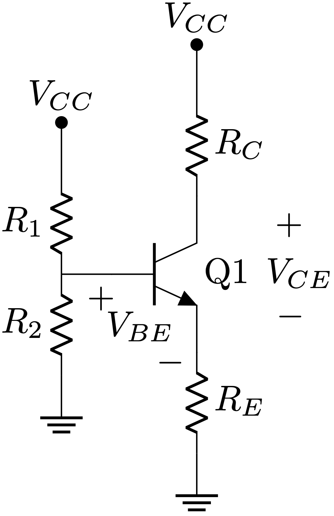
With this simplification, we come up with the following circuit:
To compute the base current, we are going to compute the KCL on the loop between \(V_{TH}\) and the emitter.\[V_{TH} – I_B R_{TH} – V_{BE} – I_E R_E = 0\]Since we are assuming we are in active mode, we can identify \(I_E = \left(\beta + 1\right) I_B\)
\[V_{TH} – I_B R_{TH} – V_{BE} – \left(\beta + 1\right) I_B R_E = 0\]
\[I_B = \frac{V_{TH} – V_{BE}}{\left(\beta + 1\right) R_E + R_{TH}}\]Now, in order to compute the collector’s voltage:
\[V_C = V_{CC} – I_C R_C = V_{CC} – \beta I_B R_C\]And for the emitter’s voltage:
\[V_E = I_E R_E = \left(\beta + 1\right) I_B R_E\]
Assigning values to all components we can work out a practical example:
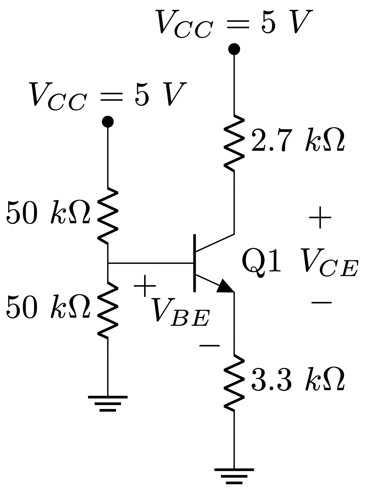
Assuming \(\beta = 100\):
\[V_{TH} = \frac{50~k\Omega}{50~k\Omega + 50~k\Omega} 5 V = 2.5~V\]
\[R_{TH} = \frac{50~k\Omega \cdot 50~k\Omega}{50~k\Omega + 50~k\Omega} = 25~k\Omega\]
\[I_B = \frac{2.5~V – 0.7~V}{\left(100 + 1\right) \cdot 3.3~k\Omega + 25~k\Omega} = 5~\mu A\]
\[V_C = 5~V – 100 \cdot 5~\mu A \cdot 2.7~k\Omega = 3.65~V\]
\[V_E = \left(100 + 1\right) \cdot 5~\mu A \cdot 3.3~k\Omega =1.66~V \]
With this, \(V_{CE}\) is 2 V approx. Therefore, the condition of \(V_{CE} \geq 0.3 \) is held and it can be said that the BJT is working on active mode.
Small-signal input and output DC impedances of a emitter follower
Now the we understand how to analyse this circuit, we may wonder how we can choose the resistors values. Since we usually design our circuits to have a high input impedance and a low output impedance to avoid loading issues between previous and next stages connected to our circuit, or putting it more synthetically, \(Z_{out} \ll Z_{in}\) (where a factor of 10 is a comfortable rule of thumb), we need to figure out what relationship \(R_1\) \(R_2\) and \(R_E\) may have.
If we assign the emitter as the output of our circuit, which stands as as an emitter follower (actually we wouldn’t need \(R_C\) for this configuration to work), then we can compute the output impedance using the following rationale:
If we make a voltage change in the base \(\Delta V_B\), the change at the emitter is \(\Delta V_E = \Delta V_B\). This is because the voltage on the emitter of an emitter follower, follows the voltage at the base. Not really surprising judging by its name 😉 .
At the same time, the current on the emitter will be:
\[ \Delta I_E = \frac{\Delta V_B}{R_E} \]
Since we are assuming the emitter follower is working on active mode and this implies that \(I_E = \left(\beta + 1\right) I_B\), we can extrapolate that:
\[ \Delta I_B = \frac{1}{\beta + 1} \Delta I_E = \left\{ \xrightarrow[]{\Delta I_E = \frac{\Delta V_B}{R_E}} \right\} = \frac{\Delta V_B}{R_E\left(\beta + 1\right)} \]
The input impedance would be \(\Delta V_B / \Delta I_B\), which can be extracted from previous expression as:
\[Z_{in} = \frac{\Delta V_B}{\Delta I_B} = R_E\left(\beta + 1\right) \]
We can compute \(\Delta V_E/ \Delta I_E\) knowing that a variation on \(\Delta V_E\) is the same as a variation on \(\Delta V_B\). Also, the variation of \(\Delta I_E = \left(\beta + 1\right) \Delta I_B = \left(\beta + 1\right) \frac{\Delta V_B}{R_{th}}\). Putting both things together:
\[Z_{out} = \frac{\Delta V_E}{\Delta I_E} = \frac{\Delta V_B}{\Delta V_B \left(\beta + 1\right)}{ R_{th}} = \frac{R_{th}}{\beta + 1}\]
Python script to get BJT values
If you want to play with different values to see if they sets your BJT into active mode, you can use this ridiculously simple Python snippet:
r1 = 50e3
r2 = 50e3
rc = 2.7e3
re = 3.3e3
rth = r1*r2/(r1+r2)
vcc = 5
vth = vcc * r2/(r2 + r1)
vbe = 0.7
beta = 100
vce_min = 0.3

ib = (vth - vbe)/((beta + 1) * re + rth)
vb = vth - ib * rth
vc = vcc - rc * beta * ib
ve = (beta + 1) * ib * re

vce = vc - ve

print(f"vth = {vth} V\nib = {ib * 1000} mA\nvb = {vb} V\nvc = {vc} V\nve = {ve} V\nvce = {vce} > {vce_min} V? {vce > vce_min}")
Output:
vth = 2.5 V
ib = 0.005023723137036003 mA
vb = 2.3744069215740997 V
vc = 3.6435947530002792 V
ve = 1.6744069215741 V
vce = 1.9691878314261793 > 0.3 V? TrueThe LaTeX code used to generate this post diagrams is:
\begin{circuitikz}
	\ctikzset{bipoles/resistor/height=0.15}
	\ctikzset{bipoles/resistor/width=0.4}
	\ctikzset{transistors/arrow pos=end}
	\draw (0,0) to[R,l=$R_1$] ++(0, 1.0) to[short, -*] ++(0,0.5) node[above]{$V_{CC}$};
	\draw (0,0) to[R,l_=$R_2$] ++(0, -1.0) node[ground]{};
	\draw (0,0) to[short] ++(0.5,0) coordinate(bjt_base);
	\draw (bjt_base)  node[npn, anchor=B](Q1){Q1};
	\draw (Q1.E) to[R, l=$R_E$] ++(0, -1.0) node[ground]{};
	\draw (Q1.C) to[R, l_=$R_C$] ++(0, 1.0) to[short, -*] ++(0, 0.5) node[above]{$V_{CC}$};
	\draw (Q1) node[anchor=north east, yshift=-7, xshift=-3]{$V_{BE}$};
	\draw (Q1.B) node[below, xshift=-3]{$+$};
	\draw (Q1.E) node[left, yshift=-3]{$-$};
	\draw (Q1.C) node[above, xshift=26, yshift=-15]{$+$};
	\draw (Q1.E) node[right, xshift=19, yshift=10]{$-$};
	\draw (Q1) node[anchor=north west, yshift=8, xshift=16]{$V_{CE}$};
\end{circuitikz}
\begin{circuitikz}
	\ctikzset{bipoles/resistor/height=0.15}
	\ctikzset{bipoles/resistor/width=0.4}
	\ctikzset{transistors/arrow pos=end}
	\draw (0,0) -- (0,-0.5) to[vsource, l_=$V_{TH}$] +(0, -1.0) coordinate(Vcc_bottom) node[ground]{};
	\draw (0,0) to[R, l=$R_{TH}$] ++(1.0,0) coordinate(bjt_base);
	\draw (bjt_base)  node[npn, anchor=B](Q1){Q1};
	\draw (Q1.E) to[R, l=$R_E$] ++(0, -1.0) node[ground]{};
	\draw (Q1.C) to[R, l_=$R_C$] ++(0, 1.0) to[short, -*] ++(0, 0.5) node[above]{$V_{CC}$};
	\draw (Q1) node[anchor=north east, yshift=-7, xshift=-3]{$V_{BE}$};
	\draw (Q1.B) node[below, xshift=-3]{$+$};
	\draw (Q1.E) node[left, yshift=-3]{$-$};
	\draw (Q1.C) node[above, xshift=26, yshift=-15]{$+$};
	\draw (Q1.E) node[right, xshift=19, yshift=10]{$-$};
	\draw (Q1) node[anchor=north west, yshift=8, xshift=16]{$V_{CE}$};
\end{circuitikz}