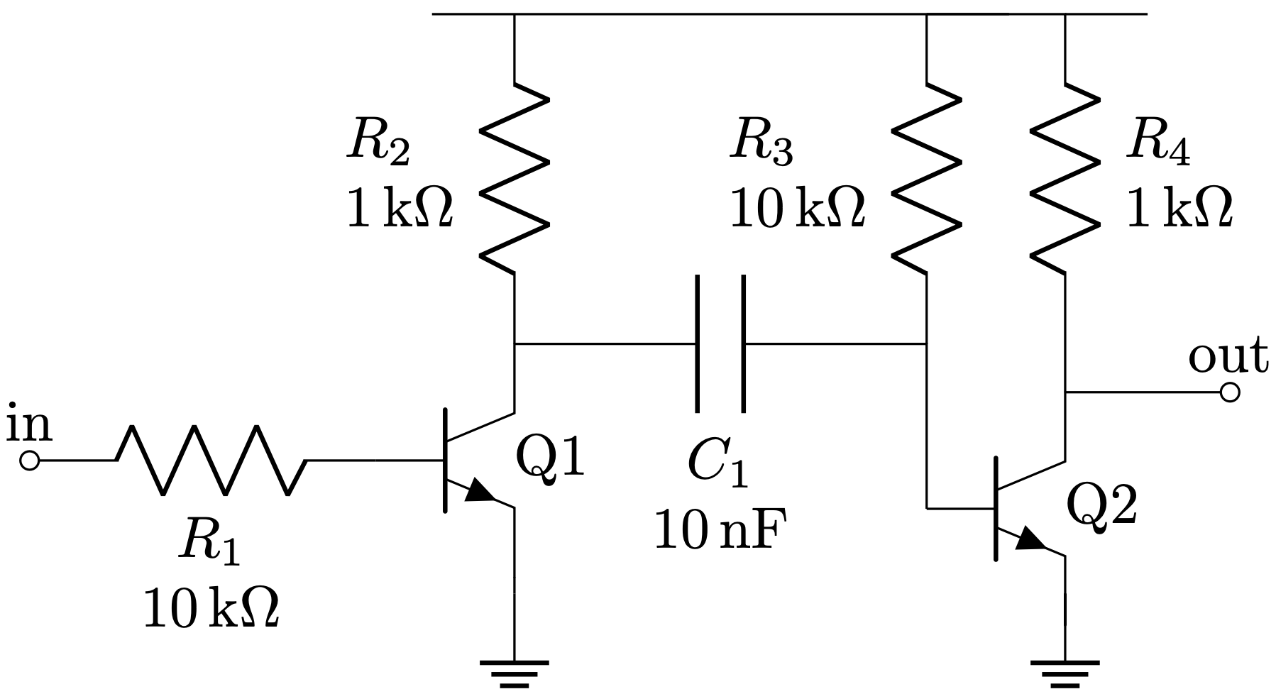
The following circuit is known as a Schmitt trigger, implemented with BJT transistors. The main purpose of a Schmitt trigger is to generate a digital signal, which stated in other words is a signal whose only possible values are \(V_{cc}\) (logic 1) or ground (logic 0). The original analog signal can vary slowly in time so that the transition periods from high/low to low/high might not be fast enough. This circuit will act as a comparator with hysteresis whose thresholds for setting the output high or low will be defined by the design parameters.
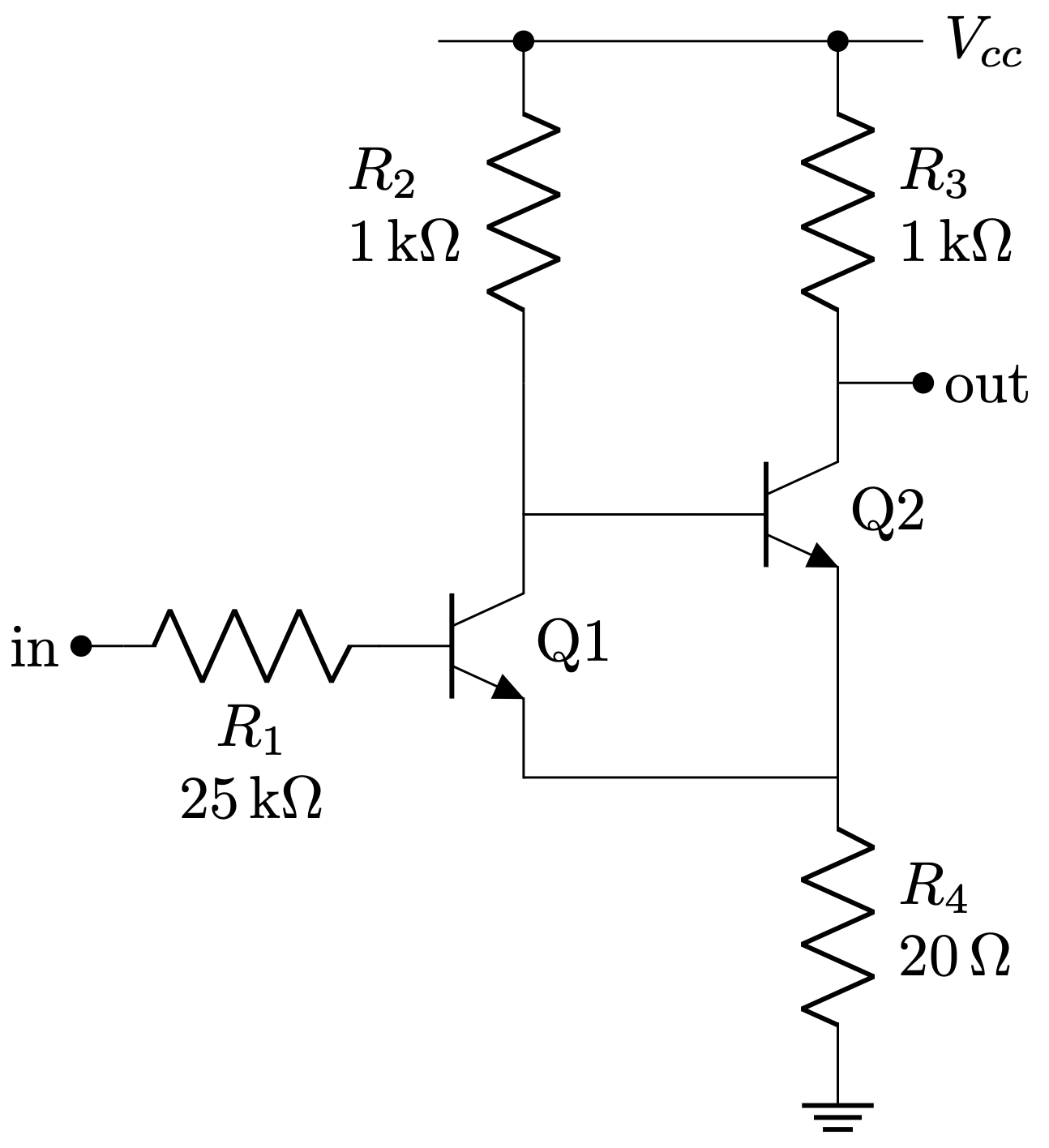
Throughout the analysis we are going to consider for simplicity a voltage \(V_{be} = 0.6~V\) for the NPN to leave cut off and \(V_{ce} = 0.0~V\) when in saturation.

A couple of details that can be extracted from here:
- By having a voltage able to take \(Q_1\) into saturation, the output goes to \(V_{cc}\).
- In order to get \(Q_1\) cut off, we need to drop \(in\) approximately \(100~mV\) higher than the \(v_{be}\) voltage, i.e., \(Q_1\) would cut off around \(in \approx 0.7~V\).
Therefore, let’s see what happens when from \(in = 5~V\) we drop \(in\) to \(0.7~V\).
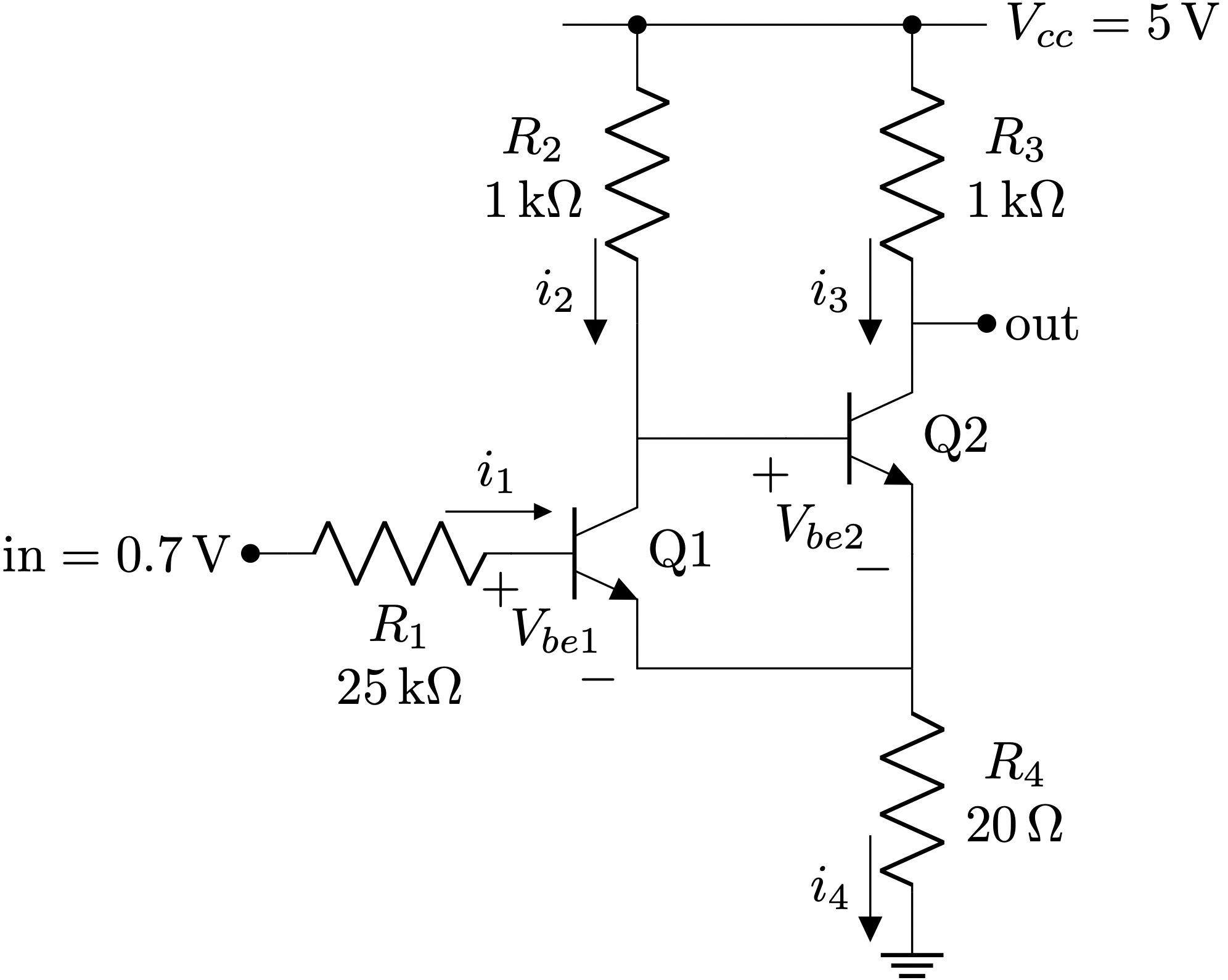
However, now that \(in = 0.7~V\), \(Q_1\) starts to stop driving current.
This makes the voltage at \(V_{b2}\) to rise due to a lower voltage drop across \(R_2\) and \(Q_2\) enters in saturation.
Since \(Q_2\) is in saturation, \(v_{be} = 0.6~V\)
In order to compute the currents going through the circuit in this state we can perform a mesh analysis taking into account the \(V_{BE}\) voltage between the base and the emitter and considering \(V_{CE} = 0\).
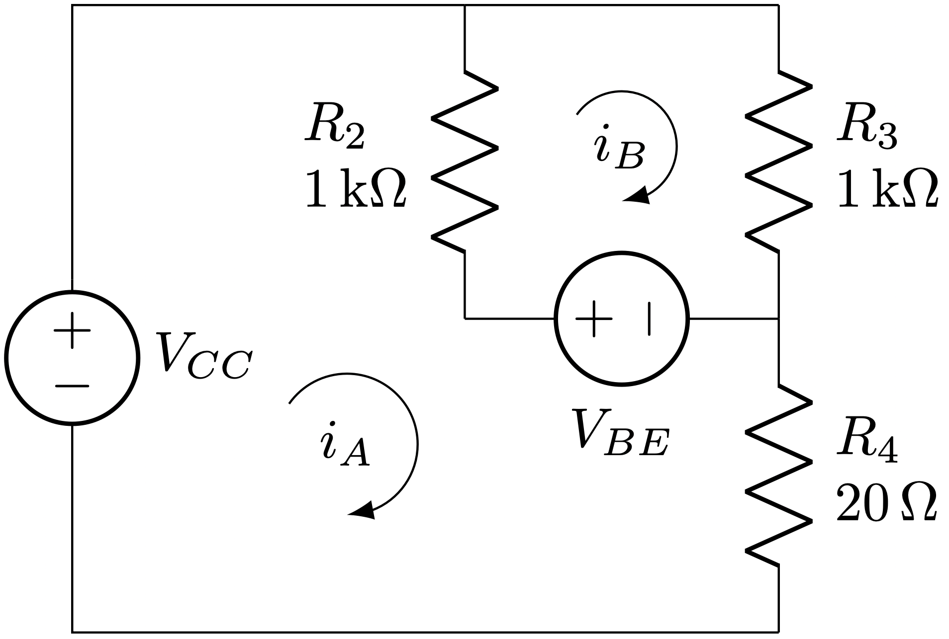
\[-V_{cc} + \left(R_2 + R_4\right)\cdot i_A + V_{be} – R_2\cdot i_B = 0\] \[-V_{be} – R_2\cdot i_A + \left(R_2 + R_3\right)\cdot i_B = 0\] Which can be written in matrix form as:\[\begin{pmatrix}
R_2 + R_4 & -R_2 \\
-R_2 & R_2 + R_3 \\
\end{pmatrix}
\begin{pmatrix}
i_A\\
i_B\\
\end{pmatrix} =
\begin{pmatrix}
V_{cc} – V_{be} \\
V_{be}
\end{pmatrix}\] Solving this equation as \(X = A^{-1} B\) we get that:\[i_A = 9.03~mA,~~ i_B = 4.81~mA\]With these current values, the voltage at the Q2 emitter is: \[V_{e} = i_A \cdot R_4 = 9.03~mA \cdot 20~\Omega = 180.6~mV\]
Again, what we can extract from these results is:
- By having a voltage able to set \(Q_1\) cut off, the output goes to \(180~mV\), which in most of the digital families such as TTL or CMOS can be safely considered as a logic 0.
- In order to get \(Q_1\) in saturation again, we need to increase \(in\) approximately \(180~mV\) above the \(v_{be} = 0.6\) voltage, i.e., \(Q_1\) would saturate around \(in \approx 0.78~V\).
So as we can see the circuit has hysteresis since thresholds for low to high and high to low are placed at different input voltages. This effect avoids having potentially multiple toggles at the output when the input voltage is near the threshold if the threshold would have been the same in both cases (low to high and high to low). Finally, the hysteresis voltage \(\Delta V\) can be approximated as \(\Delta V = \frac{R4}{R3} \cdot V_{cc}\).
LaTeX used to generate this article’s images:
\begin{circuitikz}
	\ctikzset{transistors/arrow pos=end}
	\draw (0,0) node[npn] (Q1){Q1};
	\draw (Q1.B) to[R, l2=$R_1$ and \SI{25}{\kilo\ohm}, l2 halign=c] ++(-1.5, 0) coordinate(in);
	\draw (in) to[short, -*] ++(-0.25,0) node[left]{in};
	\draw (Q1.C) -- +(1,0) node[npn, anchor=B](Q2){Q2} ;
	\draw (Q2.E) -- (Q2.E |- Q1.E);
	\draw (Q1.E) -- (Q1.E -| Q2.E);
	\draw (Q2.C) to[short, -*] +(0.5, 0) node[right]{out};
	\draw (Q1.E -| Q2.E) -- +(0, -0.25) to[R, l2=$R_4$ and \SI{20}{\ohm}] ++(0, -1.5) node[ground]{};
	\draw (Q1.C) -- (Q1.C |- Q2.C);
	\draw (Q1.C |- Q2.C)  to[R, l2=$R_2$ and \SI{1}{\kilo\ohm}, -*] ++(0, 2) coordinate(R2_top);
	\draw (Q2.C) to[R, l2_=$R_3$ and \SI{1}{\kilo\ohm}, -*] ++(0, 2) coordinate (R3_top);
	\draw (R3_top) -- (R2_top) -- +(-0.5, 0);
	\draw (R3_top) -- +(0.5, 0)  node[right]{$V_{cc}$};
\end{circuitikz}
\begin{circuitikz}
\ctikzset{transistors/arrow pos=end}
\draw (0,0) node[npn] (Q1){Q1};
\draw (Q1.B) to[R, l2=$R_1$ and \SI{10}{\kilo\ohm}, l2 halign=c, f<_=\SI{430}{\micro\ampere}, current arrow scale=24] ++(-1.5, 0) coordinate(in);
\draw (Q1.B) node[below, xshift=-2]{$+$};
\draw (Q1.E) node[anchor=south east, yshift=-9]{$-$};
%\draw ($(Q1.B)!0.5!(Q1.E)$) coordinate(vbe_label);
%\draw (vbe_label) node[yshift=-3, xshift=-2]{$V_{be1}$};
\draw (Q1) node[anchor=north east, yshift=-7, xshift=-3]{$V_{be1}$};
\draw (in) to[short, -*] ++(-0.25,0) node[left]{$\text{in} = \SI{5}{\volt}$};
\draw (Q1.C) -- +(1,0) node[npn, anchor=B](Q2){Q2} ;
\draw (Q2.E) -- (Q2.E |- Q1.E);
\draw (Q1.E) -- (Q1.E -| Q2.E);
\draw (Q2.C) to[short, -*] +(0.5, 0) node[right]{out};
\draw (Q2.B) node[below, xshift=-3]{$+$};
\draw (Q2.E) node[left, yshift=-3]{$-$};
\draw (Q2) node[anchor=north east, yshift=-9, xshift=-5]{$V_{be2}$};
\draw (Q1.E -| Q2.E) -- +(0, -0.25) coordinate(R4_top) to[R, l2=$R_4$ and \SI{20}{\ohm}, f_=\SI{5.43}{\milli\ampere}, l2 halign=c] ++(0, -1.5) node[ground]{};
\draw (Q1.C) -- (Q1.C |- Q2.C);
\draw (Q1.C |- Q2.C) to[R, l2=$R_2$ and \SI{1}{\kilo\ohm}, -*, f<^=\SI{4.9}{\milli\ampere}, l2 halign=c] ++(0, 2) coordinate(R2_top);
\draw (Q2.C) to[R, l2_=$R_3$ and \SI{1}{\kilo\ohm}, -*, f<^=\SI{0}{\milli\ampere}, l2 halign=c] ++(0, 2) coordinate (R3_top);
\draw (R3_top) -- (R2_top) -- +(-0.5, 0);
\draw (R3_top) -- +(0.5, 0) node[right]{$V_{cc}=\SI{5}{\volt}$};
\end{circuitikz}\begin{circuitikz}
\draw (0, 0) to[R, l2_=$R_2$ and \SI{1}{\kilo\ohm}] +(0, -2) coordinate(R2_bottom);
\draw (R2_bottom) to[vsource, l_=$V_{BE}$] +(2, 0) coordinate(QB);
\draw (R2_bottom -| QB) to[R, l2_=$R_3$ and \SI{1}{\kilo\ohm}] +(0, 2) coordinate(R3_top);
\draw (QB) to [R, l=$R_4$, l2=$R_4$ and \SI{20}{\ohm}] +(0, -2) coordinate (R4_bottom);
\draw (0,0) -- (R3_top);
\draw (0,0) -- (-2.5, 0) -- (-2.5, -1.75);
\draw (-2.5, -1.75) to[vsource, l=$V_{CC}$] +(0, -1.0) coordinate(Vcc_bottom) -- (R4_bottom -| Vcc_bottom) -- (R4_bottom);
\draw [Latex-] (1.0,-1.25) coordinate(loop) node [anchor=center, yshift=10] {$i_B$} arc (-90:145:3.5mm);
\draw [Latex-] (-0.75,-3.25) coordinate(loop) node [anchor=center, yshift=13] {$i_A$} arc (-90:145:4.5mm);
\end{circuitikz}