1. Install XAMPP with PHP 7.4.33

2. In the httpd.conf file, replace daemon with your name when in User daemon –> User tesla

3. In /Applications/XAMPP/xamppfiles/phpmyadmin, set tmp file with 777 permissions: sudo chmod -R 777 tmp

4. Download built crater from https://crater.financial/open-source (not github release). Copy it at /Applications/XAMPP/xamppfiles/htdocs.

5. Set writing permissions with chmod -R 777 /Applications/XAMPP/xamppfiles/htdocs/crater

6. Access localhost/phpmyadmin. Create a new user called `crater` with all permissions and access to localhost.

7. Creater an empty database called crater.

7. Configure the Apache server to point to crater/public folder:
DocumentRoot "/Applications/XAMPP/xamppfiles/htdocs/crater/public"

8. Open /Applications/XAMPP/xamppfiles/etc/php.ini, look for «[Pcre]» and paste in the section pcre.jit=0

8. Restart Apache server and turn on MySQL server.

9. Access localhost. Crater installation page should appear. Follow steps to get Crater working.


Laplace analysis

\[H\left(s\right) = – \frac{\frac{1}{sC}}{R} = – \frac{1}{sRC}\]

Bilinear (or Tustin) transform

The Laplace transfer function can be approximated into the Z domain using the bilinear or tustin transform. The mapping between Laplace and Z domain using the first order approximation of the bilinear transform is:

\[s = \frac{2}{T_s} \frac{z-1}{z+1}\]

Replacing \(s\) with previous expression, we can get the following transfer function in the Z domain:

\[H\left( z \right) =H\left(s\right)\bigg|_{s = \frac{2}{T} \frac{z – 1}{z + 1}} = – \frac{1}{\frac{2}{T_s } \frac{z-1}{z+1} RC  } = -\frac{z+1}{\frac{2}{T_s} RC \left(z – 1\right)} = -\frac{T_s}{2RC} \frac{z+1}{z-1}\]

The transfer function can now be transformed into a finite differences equation:
\[\frac{Y\left(z\right)}{X\left(z\right)} = -\frac{T_s}{2RC} \frac{z+1}{z-1} = -\frac{T_s}{2RC} \frac{1 + z^{-1}} {1 – z^{-1}}\]

\[Y\left(z\right) \left(1 – z^{-1} \right) = -\frac{T_s}{2RC} \left(1 + z^{-1}\right)\]

\[y[n] – y[n-1] = -\frac{T_s}{2RC} \left(x[n] + x[n-1]\right)\]

\[y[n] = -\frac{T_s}{2RC} \left( x[n] + x[n-1] \right) + y[n-1] \]

Python implementation

from scipy import signal
import numpy as np
import matplotlib.pyplot as plt

# Sampling frequency
fs = 1e4
# Sampling period
Ts = 1/fs

# Amplitude
A = 2.0
# Number of periods to represent
n_periods = 1
# Sine frequency (Hz)
f = 200
# Total time to represent
t_total_time = n_periods * 1/f

# Resistance (Ohms)
R = 1e3
# Capacitance (Farads)
C = 1e-6

def integrate(current_in, prev_in, prev_out):
    """
        Perform sample integration on OA integrator circuit
    """
    return Ts/(2*R*C) * (current_in + prev_in) + prev_out


# Time array
t = np.arange(0, t_total_time, Ts)
# Sine signal
sine = A * np.sin(2*np.pi*f*t)
# Constant signal
const = A * np.ones(len(t))

# Initialize output arrays to 0
out_sine = np.zeros(len(t))
out_const = np.zeros(len(t))

# Check that length is the same. Otherwise, for loop below
# has to be split
assert(len(out_sine) == len(out_const))

# Pass input signal through integrator (compute output values)
for n in range(1, len(out_sine)):
    out_sine[n]  = integrate(sine[n], sine[n-1], out_sine[n-1])
    out_const[n] = integrate(const[n], const[n-1], out_const[n-1])

# Plot input and output signals
fig = plt.figure()
plt.subplot(211)
plt.plot(t, sine)
plt.title('Input signal (sine)')
plt.ylabel('Amplitude')
plt.xlabel('Time (s)')
plt.grid(True)
plt.subplot(212)
plt.title('Output signal')
plt.plot(t, out_sine)
plt.xlabel('Time (s)')
plt.ylabel('Amplitude')
plt.grid(True)
fig.tight_layout()
plt.savefig('sine_integration.png', dpi=300)
plt.show()

fig = plt.figure()
plt.subplot(211)
plt.plot(t, const)
plt.title('Input signal (constant)')
plt.ylabel('Amplitude')
plt.xlabel('Time (s)')
plt.grid(True)
plt.subplot(212)
plt.title('Output signal')
plt.plot(t, out_const)
plt.xlabel('Time (s)')
plt.ylabel('Amplitude')
plt.grid(True)
fig.tight_layout()
plt.savefig('const_integration.png', dpi=300)
plt.show()

LaTeX code used to generate circuit schematic

\begin{circuitikz} []	
	\ctikzset{resistors/scale=0.7, capacitors/scale=0.6}
        \draw (0,0)  node[left]{in} to[short, *-] ++(0.5, 0)  to[R, l=R] ++(1.5,0)  coordinate(inm) node[op amp, anchor=-](OA){};
	\draw (inm) -- ++(0, 1.5)  coordinate(C_left) to[C, l=C] (C_left -| OA.out) -- (OA.out) to[short, -*] ++(0.5, 0) node[right]{out};
	\draw (OA.+) -- ++(0, -0.5) node[ground]{};
\end{circuitikz}

\begin{circuitikz} []	
	\ctikzset{resistors/scale=0.7, capacitors/scale=0.6}
        \draw (0,0)  node[left]{in} to[short, *-] ++(0.5, 0)  to[R, l=R] ++(1.5,0)  coordinate(inm) node[op amp, anchor=-](OA){};
	\draw (inm) -- ++(0, 1.5)  coordinate(C_left) to[C, l=$\frac{1}{sC}$] (C_left -| OA.out) -- (OA.out) to[short, -*] ++(0.5, 0) node[right]{out};
	\draw (OA.+) -- ++(0, -0.5) node[ground]{};
\end{circuitikz}

In this post we are going to discuss the DC analysis of Bipolar Junction Transistors (BJT).

BJT’s can work in three modes:

  1. Cut-off: the transistor is not driving any current through the emitter and the collector.
  2. Active: the current on the collector is \(\beta\) times the current on the base \(I_C = \beta I_B\) and \(I_E = \left( \beta + 1\right) I_B\). This is the usual mode of operation when trying to use the transistor as an amplifier. In this mode, the base-emitter voltage will be around 0.7 V (\(V_{BE} \approx 0.7~V\)) and it is required that the condition of having a collector-emitter voltage \(V_{CE}\) greater than 0.3 V (\( V_{CE} \geq 0.3~V\)) is held. If this condition is not held, then the BJT might be in saturation mode.
  3. Saturation: in this mode, the transistor is no longer able to provide more current for the given base current. Therefore it doesn’t matter if we increase the base current that the collector current will remain constant. In this case, \(I_C = \beta_{forced} I_B\) where \(\beta_{forced} < \beta\).

In order to identify in which region we are setting the transistor, we can make an assumption, compute the voltages on base, emitter and collector and verify if the assumption was correct. Let’s see an example in which the BJT’s base is biased using the simplest approach possible: a voltage divider.

In this circuit, the base voltage is given by the resistor divider \(R_1\) and \(R_2\). In order to simplify the analysis, although it is not actually necessary, we can compute the Thevening equivalent of the circuit connect on the left hand side of the BJT’s base. The Thevenin’s equivalent voltage will be \(V_{TH} = \frac{R_2}{R_1 + R_2} V_{CC}\) whereas the Thevenin’s equivalent resistance would be the parallel of \(R_1\) and \(R_2\): \(R_{TH} = R_1 || R_2 = \frac{R_1 R_2}{R_1 + R_2}\)

With this simplification, we come up with the following circuit:

Now we can start computing the base current, the emitter voltage and the collector voltage. To do so, we are going to assume that the BJT is in active mode, which means that \(I_C = \beta I_B\) and \(V_{BE} \approx 0.7~V\). In order to verify that we are in active mode, after having computed all circuit values with using this assumption, it must be held that \(V_{CE} \geq 0.3~V\).
To compute the base current, we are going to compute the KCL on the loop between \(V_{TH}\) and the emitter.\[V_{TH} – I_B R_{TH} – V_{BE} – I_E R_E = 0\]Since we are assuming we are in active mode, we can identify \(I_E = \left(\beta + 1\right) I_B\)
\[V_{TH} – I_B R_{TH} – V_{BE} – \left(\beta + 1\right) I_B R_E = 0\]
\[I_B = \frac{V_{TH} – V_{BE}}{\left(\beta + 1\right) R_E + R_{TH}}\]Now, in order to compute the collector’s voltage:
\[V_C = V_{CC} – I_C R_C = V_{CC} – \beta I_B R_C\]And for the emitter’s voltage:
\[V_E = I_E R_E = \left(\beta + 1\right) I_B R_E\]

Assigning values to all components we can work out a practical example:

Assuming \(\beta = 100\):

\[V_{TH} = \frac{50~k\Omega}{50~k\Omega + 50~k\Omega} 5 V = 2.5~V\]

\[R_{TH} = \frac{50~k\Omega \cdot 50~k\Omega}{50~k\Omega + 50~k\Omega} = 25~k\Omega\]

\[I_B = \frac{2.5~V – 0.7~V}{\left(100 + 1\right) \cdot 3.3~k\Omega + 25~k\Omega} = 5~\mu A\]

\[V_C = 5~V – 100 \cdot 5~\mu A \cdot  2.7~k\Omega = 3.65~V\]

\[V_E = \left(100 + 1\right) \cdot 5~\mu A \cdot 3.3~k\Omega =1.66~V \]

With this, \(V_{CE}\) is 2 V approx. Therefore, the condition of \(V_{CE} \geq 0.3 \) is held and it can be said that the BJT is working on active mode.

Small-signal input and output DC impedances of a emitter follower

Now the we understand how to analyse this circuit, we may wonder how we can choose the resistors values. Since we usually design our circuits to have a high input impedance and a low output impedance to avoid loading issues between previous and next stages connected to our circuit, or putting it more synthetically, \(Z_{out} \ll Z_{in}\) (where a factor of 10 is a comfortable rule of thumb), we need to figure out what relationship \(R_1\) \(R_2\) and \(R_E\) may have.

If we assign the emitter as the output of our circuit, which stands as as an emitter follower (actually we wouldn’t need \(R_C\) for this configuration to work), then we can compute the output impedance using the following rationale:

If we make a voltage change in the base \(\Delta V_B\), the change at the emitter is \(\Delta V_E = \Delta V_B\). This is because the voltage on the emitter of an emitter follower, follows the voltage at the base. Not really surprising judging by its name 😉 .
At the same time, the current on the emitter will be:
\[ \Delta I_E = \frac{\Delta V_B}{R_E} \]

Since we are assuming the emitter follower is working on active mode and this implies that \(I_E = \left(\beta + 1\right) I_B\), we can extrapolate that:
\[ \Delta I_B = \frac{1}{\beta + 1} \Delta I_E = \left\{ \xrightarrow[]{\Delta I_E = \frac{\Delta V_B}{R_E}} \right\} = \frac{\Delta V_B}{R_E\left(\beta + 1\right)} \]

The input impedance would be \(\Delta V_B / \Delta I_B\), which can be extracted from previous expression as:
\[Z_{in} = \frac{\Delta V_B}{\Delta I_B} = R_E\left(\beta + 1\right) \]

We can compute \(\Delta V_E/ \Delta I_E\) knowing that a variation on \(\Delta V_E\) is the same as a variation on \(\Delta V_B\). Also, the variation of \(\Delta I_E = \left(\beta + 1\right) \Delta I_B = \left(\beta + 1\right) \frac{\Delta V_B}{R_{th}}\). Putting both things together:

\[Z_{out} = \frac{\Delta V_E}{\Delta I_E} = \frac{\Delta V_B}{\Delta V_B \left(\beta + 1\right)}{ R_{th}} = \frac{R_{th}}{\beta + 1}\]

Python script to get BJT values

If you want to play with different values to see if they sets your BJT into active mode, you can use this ridiculously simple Python snippet:

r1 = 50e3
r2 = 50e3
rc = 2.7e3
re = 3.3e3
rth = r1*r2/(r1+r2)
vcc = 5
vth = vcc * r2/(r2 + r1)
vbe = 0.7
beta = 100
vce_min = 0.3

ib = (vth - vbe)/((beta + 1) * re + rth)
vb = vth - ib * rth
vc = vcc - rc * beta * ib
ve = (beta + 1) * ib * re

vce = vc - ve

print(f"vth = {vth} V\nib = {ib * 1000} mA\nvb = {vb} V\nvc = {vc} V\nve = {ve} V\nvce = {vce} > {vce_min} V? {vce > vce_min}")

Output:

vth = 2.5 V
ib = 0.005023723137036003 mA
vb = 2.3744069215740997 V
vc = 3.6435947530002792 V
ve = 1.6744069215741 V
vce = 1.9691878314261793 > 0.3 V? True

BJT biasing – EveryCircuit


The LaTeX code used to generate this post diagrams is:

\begin{circuitikz}
	\ctikzset{bipoles/resistor/height=0.15}
	\ctikzset{bipoles/resistor/width=0.4}
	\ctikzset{transistors/arrow pos=end}
	\draw (0,0) to[R,l=$R_1$] ++(0, 1.0) to[short, -*] ++(0,0.5) node[above]{$V_{CC}$};
	\draw (0,0) to[R,l_=$R_2$] ++(0, -1.0) node[ground]{};
	\draw (0,0) to[short] ++(0.5,0) coordinate(bjt_base);
	\draw (bjt_base)  node[npn, anchor=B](Q1){Q1};
	\draw (Q1.E) to[R, l=$R_E$] ++(0, -1.0) node[ground]{};
	\draw (Q1.C) to[R, l_=$R_C$] ++(0, 1.0) to[short, -*] ++(0, 0.5) node[above]{$V_{CC}$};
	\draw (Q1) node[anchor=north east, yshift=-7, xshift=-3]{$V_{BE}$};
	\draw (Q1.B) node[below, xshift=-3]{$+$};
	\draw (Q1.E) node[left, yshift=-3]{$-$};
	\draw (Q1.C) node[above, xshift=26, yshift=-15]{$+$};
	\draw (Q1.E) node[right, xshift=19, yshift=10]{$-$};
	\draw (Q1) node[anchor=north west, yshift=8, xshift=16]{$V_{CE}$};
\end{circuitikz}
\begin{circuitikz}
	\ctikzset{bipoles/resistor/height=0.15}
	\ctikzset{bipoles/resistor/width=0.4}
	\ctikzset{transistors/arrow pos=end}
	\draw (0,0) -- (0,-0.5) to[vsource, l_=$V_{TH}$] +(0, -1.0) coordinate(Vcc_bottom) node[ground]{};
	\draw (0,0) to[R, l=$R_{TH}$] ++(1.0,0) coordinate(bjt_base);
	\draw (bjt_base)  node[npn, anchor=B](Q1){Q1};
	\draw (Q1.E) to[R, l=$R_E$] ++(0, -1.0) node[ground]{};
	\draw (Q1.C) to[R, l_=$R_C$] ++(0, 1.0) to[short, -*] ++(0, 0.5) node[above]{$V_{CC}$};
	\draw (Q1) node[anchor=north east, yshift=-7, xshift=-3]{$V_{BE}$};
	\draw (Q1.B) node[below, xshift=-3]{$+$};
	\draw (Q1.E) node[left, yshift=-3]{$-$};
	\draw (Q1.C) node[above, xshift=26, yshift=-15]{$+$};
	\draw (Q1.E) node[right, xshift=19, yshift=10]{$-$};
	\draw (Q1) node[anchor=north west, yshift=8, xshift=16]{$V_{CE}$};
\end{circuitikz}

The UVM spins around the concept of abstracting the data that is sent and received from the DUT. Data abstraction allows to create and handle complex structures able to describe elaborated scenarios. For instance, we can model a burst I2C writing of 100 bytes without worrying too much about how that is going to be actually implemented. Each byte could be respresented as a transaction and from the TLM perspective we would only need to focus on the meaningful data required for fully describing the operation. Since in UVM each environment component is in charge of different actions (driving, monitoring, arbitring, etc.) a communication mechanism is required for transactions to be sent between the environment components. UVM provides TLM API and classes to do allow such communication.

In this sort of communication there is always a producer and a consumer. However, there are cases where we may want to send the transactions regardless the number of consumers (0, 1 or many). That can be implemented using analysis port and exports and is not the scope of this post.

TLM ports and exports

In UVM, a port class provides functions that can be called. Because of this, it will be placed on the component that initiates the communication. As we are going to see soon, the communication can be started by either the consumer or the producer, so the port class has not to be confused with the direction of the transactions.

On the other hand, an export class specifies the implementation of the functions. Therefore, it will be placed on the component that waits for the communication to be started. Again, as in the case of the port, it gives no information per se about the direction of the transactions, only gives information about who asks for them.

The TLM API implements two different ways to control the communication flow. In the case that the communication is started by the producer, then we will need to use a put port. If it is the consumer who controls the communication, then we will use a get port.

Also, an important aspect of the ports and exports is that they require always to be connected. If they remain unconnected then you will have a `uvm_error on simulation time 0 as follows:

UVM_ERROR @ 0: uvm_test_top.env.agent.put_port [Connection Error] connection count of 0 does not meet required minimum of 1

Communication started by the producer (put)

In the producer, in order to send a uvm_object, it is necessary to call the put task on the port object.

In the consumer, we need to implement the put task where we can define what we want to do with the incoming transaction. This function will be automatically called when the producer calls the port put task.

Also, there are two different types of put ports: blocking and nonblocking.

UVM TLM blocking put port

The put method implementation is a task and therefore it can consume simulation time. If we call the put method on the producer and want to wait for the consumer to finish processing it before keep executing the producer’s code, then we need a blocking put port. By waiting for the consumer to be done with the transaction sent, we can create synchronization patterns that might be useful for our verification infrastructure.

Producer

The producer calls the put() method over the put_port.

class producer extends uvm_component;

    uvm_blocking_put_port #(packet) put_port;

    `uvm_component_utils(producer)

    function new(string name="producer", uvm_component parent);
        super.new(name, parent);
        put_port = new("put_port", this);
    endfunction

    virtual task run_phase(uvm_phase phase);
        packet pkt;
        pkt = packet::type_id::create("pkt");
        if (!pkt.randomize()) `uvm_error("NO_RND", "Couldn't randomize pkt")
        put_port.put(pkt);
    endtask : run_phase
    
endclass : producer
Consumer

The consumer executes the put() task every time the producer sends a transaction. It is important to know that in the case we need to use the transaction information at a later stage, we need to clone the object so that we hold a copy of it. Otherwise, the transaction data will change as soon as the producer generates a new object since the transaction in the consumer is passed by reference. This can lead to waste an enormous amount of time debugging why the transaction information is not matching the expected values 🙂

class consumer extends uvm_component;

    uvm_blocking_put_imp #(packet, consumer) put_export;

    `uvm_component_utils(consumer)

    function new(string name = "consumer", uvm_component parent);
        super.new(name, parent);
        put_export = new("put_export", this);
    end : new

    task put(packet pkt);
        // Called everytime the producer sends a transaction
    endtask
endclass : consumer

From the code snippet above, note that the consumer who is finally going to receive the transaction uses a uvm_blocking_put_imp object. Intuitively one can think that a uvm_blocking_put_export should be used, but that’s only used in the case of having multiple layers of communication where we need to connect an export implementation with one or more intermediate layers. Please check out the section «Multiple port/export layers» for more details.

As shown above, the put_port and put_export objects are created inside the class constructor use new and not the UVM factory.

UVM TLM nonblocking put port

If we don’t want to wait for the consumer to have processed and finished the put method before continuing with the program execution in the producer, then we can use a nonblocking put port. To do so, replace in the previous producer and consumer implementation the blocking word with nonblocking when declaring the port and export.

Communication started by the consumer (get)

In the case of being the consumer who will ask for transactions, then we will need to create an export in the producer and a port in the consumer.

UVM TLM blocking get port

class producer extends uvm_component;

    uvm_blocking_get_imp #(packet, producer) get_export;
    
    `uvm_component_utils(producer)

    function new(string name="producer", uvm_component parent);
        super.new(name, parent);
        get_export = new("get_export", this);
    endfunction

    task get(output packet pkt);
        pkt = packet::type_id::create("pkt");
        if (!pkt.randomize()) `uvm_error("NO_RND", "Couldn't randomize pkt")
    endtask : get
endclass : producer
class consumer extends uvm_component;

    uvm_blocking_get_port #(packet) get_port;

    `uvm_component_utils(consumer)

    function new(string name = "consumer", uvm_component parent);
        super.new(name, parent);
        get_port = new("get_port", this);
    end : new

    virtual task run_phase(uvm_phase phase);
        Packet pkt;
        [...]
        get_port.get(pkt);
    endtask : run_phase
endclass : consumer

UVM TLM nonblocking get port

If we don’t want to wait for the producer to send the packet before continuing with the program execution in the consumer, then we can use a nonblocking get port. To do so, again, replace in previous producer and consumer implementation the blocking word with nonblocking when declaring the port and export.

Method Blocking Nonblocking
Put
Port uvm_blocking_put_port#(tr)
uvm_nonblocking_put_port#(tr)
Export uvm_blocking_put_export#(tr)
uvm_nonblocking_put_export#(tr)
Imp uvm_blocking_put_imp#(tr, parent)
uvm_nonblocking_put_imp#(tr, parent)
Get
Port uvm_blocking_get_port#(tr)
uvm_nonblocking_get_port#(tr)
Export uvm_blocking_get_export#(tr)
uvm_nonblocking_get_export#(tr)
Imp uvm_blocking_get_imp#(tr, parent)
uvm_nonblocking_get_imp#(tr, parent)

The rest of the component implementation remains the same.

Connecting ports and exports

Both port and export have to be connected together using the connect() method. This is usually done at a higher hierarchy level, i.e., the producer and/or consumer parent. For instance, in order to connect an agent’s driver with the sequencer, the connection will be done on the agent’s class on the connect_phase().

The connect() method is implemented on the port object. Therefore, the depending on the put or get method used we will need to call the connect() over the producer or the consumer. In the example below, both cases are shown. However, bear in mind that only one actually applies for connect a TLM port and export.

class pkt_agent extends uvm_agent;

    producer prod;
    consumer cons;

    `uvm_component_utils(pkt_agent)

    [...]

    virtual function void build_phase(uvm_phase phase);
        [...]
        prod = producer::type_id::create("prod", this);
        cons = consumer::type_id::create("cons", this);
    endfunction : build_phase

    virtual function void connect_phase(uvm_phase phase);
        super.connect_phase(phase);
        // Put port/export. It does not apply on get method
        prod.put_port.connect(cons.put_export);
        // Get port/export. It does not apply on put method
        cons.get_port.connect(prod.get_export);
    endfunction : connect_phase

endclass

Multiple port/export layers

In case of having multple port/export layers, such as the case depicted below, we need to connect ports with ports and exports with exports in the highest levels of hierarchy.

When driving the transaction outwards, we will use a port. When driving the transaction inwards AND it is not the last component, we will use an export. And finally, when driving the transaction into the last component (the destination), we will use an imp (since it is the place where we will implement the put or get method).

In this case, the connections will be done as follows:

  • Port to port: child_comp.child_port.connect(parent_port)
  • Port to export: put_port_comp.put_port.connect(export_port_comp.export_port)
  • Export to export: parent_comp.parent_port.connect(child_port.export)

An example implementating the diagram above can be:

class agent_prod extends uvm_agent;

    driver drv; // Let's assume the driver has a uvm_blocking_put_port#(packet) object
    uvm_blocking_put_port put_port;

    `uvm_component_utils(agent_prod)

    function new(string name="agent_prod", uvm_component parent);
        super.new(name, parent);
        put_port = new("put_port", this);
    endfunction

    virtual function void connect_phase(uvm_phase phase);
        super.connect_phase(phase);
        drv.put_port.connect(put_port);
    endfunction : connect_phase

endclass : agent_prod

class agent_cons extends uvm_agent;

    scoreboard scb;  // Let's assume the scoreboard has a uvm_blocking_put_imp#(packet, scoreboard) object
    uvm_blocking_put_export#(packet) put_export;

    `uvm_component_utils(agent_cons)

    function new(string name="agent_cons", uvm_component parent);
        super.new(name, parent);
        put_export = new("put_export", this);
    endfunction

    virtual function void connect_phase(uvm_phase phase);
        super.connect_phase(phase);
        put_export.connect(scb.put_export);
    endfunction : connect_phase

endclass : agent_cons

class env extends uvm_env;

    agent_prod agent_port;
    agent_cons agent_exp;

    `uvm_component_utils(env)

    function new(string name, uvm_component parent);
        super.new(name, parent);
    endfunction

    function void build_phase(uvm_phase phase);
        agent_port = agent_prod::type_id::create("agent_port", this);
        agent_exp = agent_cons::type_id::create("agent_exp", this);
    endfunction

    function void connect_phase(uvm_phase phase);
        super.connect_phase(phase);
        agent_port.put_port.connect(agent_exp.put_export);
    endfunction

endclass


In Design Verification (DV), a test is a set of stimuli that exercises the Design Under Test (DUT). The purpose of the test is to verify one or more specs and/or functionalities, so to be methodogically strict, it is absolutely mandatory for the test to contain checkers that deterministically asserts whether the design is behaving as expected or not. Otherwise, the test will not have more use than help you to prepare some nice waveforms or dangerously give you a false confidence of higher functional and code coverage.

Usually, the testcase has a fixed amount of instructions or actions to do over the DUT. This might vary slightly in the case of generating randomly the data to inject into the design, but the steps to take will be known upfront. In the case of having to fulfill some functional coverage such as covergroups, it is possible that a single run won’t be able to hit all possible scenarios that a covergroup requires to get 100% coverage. One way to overcome this is to increase the number of runs of the same test to expand the hit scenarios. However, it is not always clear how many of these are going to be required in order to reach the coverage goals. You can try increasing little by little the number of runs/seeds until you get a stable figure of coverage throughout several consecutive regressions or you can take a shortcut and increase dramatically the number of seeds. Both approaches present drawbacks however. The trial and error approach requires time which you might not have. Depending on the duration of the test and the number of runs, it may take you days to figure out what is the minimum number of tests required since each regression may take several hours. On the other hand, the «all-in» strategy may be consuming unnecessary computional resources since you might be running several orders of magnitude more tests than the ones it was actually required.

The purpose of this post is to elaborate on a way in which the functional coverage can dictate whether the test must keep trying new scenarios and in turn exercising the DUT any further or stop the simulation. This can be easily done on custom made SystemVerilog testbenches, but it is way more interesting analysing how to do this using the Universal Verification Methodology (UVM) as it is the most widely used verification framework in the semiconductor industry.

The DUT, SystemVerilog testbench and UVM environment architecture presented in this post is the simplest possible. The only purpose of them is to serve as a vehicle to illustrate the mentioned approach. Also, all the code shown in this article has been uploaded to the GitHub repo uvm-cg-driven in case you just want to dive directly into the code.

The DUT (dut.sv)

The DUT is a dummy, empty module with 3 input ports: address, data and clock. In this case study we are only interested on generating the stimuli reaching this module. Therefore, the DUT is as simple as it can be.

module dut(input [3:0] addr, data, input clk);

endmodule

The testbench (tb_sim_top.sv)

The top of the simulation just contains the instatiation of the DUT, the interface required for the UVM agent and the call for UVM to start the tests.

`include "uvm_macros.svh"
import uvm_pkg::*;
import cg_driven_pkg::*;
import pkt_agent_pkg::*;

module tb;

    dut u_dut(
        .addr(pkt_if.addr),
        .data(pkt_if.data),
        .clk (pkt_if.clk)
    );

    pkt_if pkt_if();

    initial begin
        uvm_config_db#(virtual pkt_if)::set(null, "*", "pkt_vif", pkt_if);
        run_test();
    end

endmodule : tb

UVM architecture

The only existing test is called cg_driven_test. This instantiates the cg_drive_env environment object and the sequence to be run multiple times. The environment in turn instantiates a custom-made agent called pkt_agent, which is an active agent in charge of generating random values of data, addresses and clocks. It also constains a monitor that builds transaction objects from the activity seen on the interface connected to the DUT. Finally, the transactions created at the monitor are sent through an analysis port to allow any environment component to use them.

The component that uses these transactions is instantiated directly in the environment, but there is no limitation on where it can be placed as long as it has visibility of the already mentioned monitor’s analysis port. This component, called env_cg, samples the coverage and is extended from the UVM class uvm_subscriber. In essense, the uvm_subscriber class is a component with a built-in analysis export. So we can take advantage of this and connect it with the pkt_mon analysis port. Also, we can instantiate as many covergroups as we may need. The only limitation is that a uvm_subscriber component can only receive one type of transactions using the built-in analysis export. Hence, we may want to create different uvm_subscriber for every different transaction for which we want to monitor the functional coverage.

Every time that a new transaction is sent through the analysis port by the monitor, the subscriber function write() is called, so it is a nice place to call for the covergroup sample() method.

import pkt_agent_pkg::pkt_tr;

class cg_driven_subscriber extends uvm_subscriber #(pkt_tr);

    `uvm_component_utils(cg_driven_subscriber)

    pkt_tr tr;

    covergroup cg_addr;
        c_addr : coverpoint tr.addr;
    endgroup

    function new (string name = "cg_driven_subscriber", uvm_component parent);
        super.new(name, parent);
        cg_addr = new();
    endfunction : new

    virtual function void write (pkt_tr t);
        tr = t;
        `uvm_info("SUBS", $sformatf("New transaction received. Sampling coverage"), UVM_MEDIUM)
        cg_addr.sample();
    endfunction : write

endclass : cg_driven_subscriber

We can access the covergroup information from the test through the environment object. We can create a loop that can be repeated as long as the coverpoint coverage is lower than certain value. Since every time that the sequence is executed the driver generates traffic on the interface, the monitor will be able to regenerate a transaction that will eventually reach our subscriber component. Therefore, every time that the sequence finishes, the coverpoint coverage should be updated.

class cg_driven_test extends uvm_test;

    `uvm_component_utils(cg_driven_test)

    pkt_sequence seq;
    cg_driven_env env;

    function new(string name = "cg_driven_test", uvm_component parent);
        super.new(name, parent);
    endfunction : new

    function void build_phase(uvm_phase phase);
        super.build_phase(phase);
        env = cg_driven_env::type_id::create("env", this);
    endfunction : build_phase

    virtual task main_phase(uvm_phase phase);
        super.main_phase(phase);
        phase.raise_objection(this);
        `uvm_info("TEST", "Hello, World!", UVM_LOW)
        #100ns;
        seq = pkt_sequence::type_id::create("seq");
        while(env.cg_subs.cg_addr.get_inst_coverage() < 100.0) begin
            seq.start(env.pkt_agt.sqr);
            `uvm_info("CF", $sformatf("CG coverage = %0.2f %", env.cg_subs.cg_addr.get_inst_coverage()), UVM_MEDIUM);
        end
        phase.drop_objection(this);
    endtask : main_phase

endclass : cg_driven_test

Finally, we can use the method get_inst_coverage() over the coverpoint of interest, which returns a real value with the current coverage. However, we need to be aware that depending on the simulation tool used, the coverage collection might be disabled by default. For instance, in Xcelium you need to add the switch -cov U to enable the functional coverage analysis or -cov_cgsample. Please take a look at the Makefile in the repo to see the exact switches I used.

Conclusion

This is just a simple way to use covergroups inside UVM, which provides the advantage of running just the minimum number of sequences required to fulfill the coverage goals based on one or more coverpoints. This can be very convinient since you can come up with the certainty that if the test finishes, all the targeted scenarios were visited. Of course, this can not always be used and there might be cases where the multiseed approach can boost the functional coverage much quicker. Also, it is possible that due to the nature of the covergroup and the way the stimuli is generated, the test may never reach the goal figure. Therefore, this method might be useful not only to just run the minimum necessary sequences but also to identify possible problems on the way the test is generating the transactions. All in all, it seems quite reasonable to keep this approach in mind since it can work really well on simple cases and can also provide further information on the test infrastructure capabilities.

The fixed point representation consists of the representation of decimal numbers using a binary coding scheme that can’t model exactly all decimal numbers. Before getting into details, we are going to have a brief overview on different binary encondings schemes that there are.

Binary encoding using fixed point

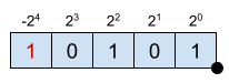
En the fixed point representation, the value of the represented number depends on the position of the 1’s and 0’z. For instance:
\[ (10010)_2 = 1 \cdot  2^4 + 0 \cdot 2^3 + 0 \cdot 2^2 + 1 \cdot 2^1 + 0 \cdot 2^0 = 18 \]
The dynamic range of this representation is given by the number of bits used. However, the addition operation using fixed point representation numbers is straigtforward.

Binary encoding using floating point

The number value doesn’t depend on the bit position. The binary number is split into 3 different parts: sign, mantissa and exponent

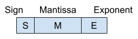
The value is computed as:

\[ \text{Value} = S \cdot M \cdot 2^{E-cte} \]

The floating point encoding provides a much greater dynamic range than the fixed point encoding. Furthermore, the resolution can be variable. Nevertheless, performing the addition operation using floating point enconding is more complex.

In order to represent integer numbers, there are two encodings that are quite used. The first one is the already mentioned fixed point encoding, whereby every bit represents a different weight of a power of 2. However, with this encoding it is not possible to represent negative numbers. To do so, the most widely used enconding is known as 2’s complement.

Fixed point encoding for unsigned integers (positive)

The encoding for N bits unsigned numbers has a range \(\left[0, 2^N -1 \right]\). In this case, the resolution is 1.

In order to compute the value of a binary number:

\[ X = \sum_{i=0}^{N-1} x_i 2^i\]

Fixed point enconding for integers with sign

The enconding for N bits numbers with sign can be done using 2’s complement. In this encoding every bit has a weight, just as in the unsigned integers. The particularity here is that the most significant bit (MSB) has a negative sign and the corresponding power of 2 weight given by its position.

\[X = -2^{-4} + 2^2 +2^0 = -11 \]

As it can be seen, the MSB has a weight of \(2^{-4}\) and a negative sign.
El 2’s complement range is \(\left[-2^{N-1}, 2^{N-1}-1 \right] \) and the resolution 1.

Comparison between numbers with sign and 2’s complement

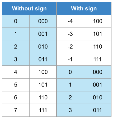
The table illustrated the representation with and without sign and its equivalence to the decimal format. In this case, N = 3 since only 3 bits are used to represent all the numbers. The range for the representation without sign is [0, 7] whereas in the case of the representation with sign is [-4, 3].

The values that are lower than \(2^{N-1} = 2^{3-1} = 2^2 = 4\) have their direct equivalency in both encodings (blue background), i.e., both are presented as \((011)_2\)

In the case of values without sign greater than \(2^{N-1}\), they should be read as:

\[ \text{Signed} = \text{Unsigned} – 2^N \]

For instance, 6 represented as unsigned is \((110)_2\). However, \((110)_2\) interpreted as a 2’s complement number is:

\[ \text{Signed} = 6 – 2^3 = 6 – 8 = -2\]

Therefore:

\[ S = \left\{\begin{matrix}
U; & U < 2^{N-1} \\
U – 2^N ;& U \geq 2^{N-1}
\end{matrix}\right.\]

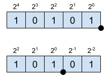
Encoding positive real numbers using fixed point

Decimal numbers can also be represented using fixed point encoding. Nonetheless, the value accuracy will depend on the number of bits used and the point position.

\[X_E = 2^{4} + 2^2 +2^0 = 21 \]
\[X_Q = 2^{2} + 2^0 +2^{-2} = 5.25 \]

The position of the point is imaginary since it not specified internally in any way. From the position of the point towards the left, the numbers represent positive powers of 2. Towards the right, negative powers of 2. The resolution of this enconding is given by the LSB.
\[ X =  \left(\sum_{i=0}^{N-1} x_i 2^i  \right) \cdot 2^{-b} \]

The notation used to describe this enconding is \([N, b]\), where \(N\) is the total number of bits and \(b\) is the number of fractional bits. For example, \([6,3]\) means 6 bits in total 3 of which are fractional. In this case, the resolution is \(2^{-3} = 0.125\).

Enconding real numbers using fixed point in 2’s complement

When representing real numbers with sign using 2’s complement, the range of the numbers is \([-2^{N-1}\cdot Q, (2^{N-1}-1) \cdot Q]\), where N is the total number of bits and Q the resolution, which is \(Q = 2^{-b}\).

\[ X = \left(-x_{N-1} 2^{N-1} + \sum_{i=0}^{N-2} x_i 2^i  \right) \cdot 2^{-b} \]

  • Example 1:
    • N = 6, b = 3, format [6,3].
    • Range: \(\left[2^{6-1}\cdot 2^{-3}, (2^{6-1}-1)\cdot 2^{-3} \right] = \left[-4, 3.875\right] \).
    • Resolution: \(2^{-3} = 0.125\).
  • Example 2:
    • N = 5, b = 2, format [5,2].
    • Range: \(\left[2^{5-1}\cdot 2^{-2}, (2^{5-1}-1)\cdot 2^{-2} \right] = \left[-4, 3.75\right] \).
    • Resolution: \(2^{-2} = 0.25\)

Encoding dynamic range

The dynamic range of an encoding is determined by the amount of numbers used to encode a range of number. For instance, in the fixed point encoding without sign, the range is \([0, \left(2^{N}-1\right)\cdot Q]\) and the resolution \(Q=2^{-b}\).

The dynamic range is the relationship between the maximum encoding difference \([-2^{N-1}, 2^{N-1} 1]\) and the encoding resolution.

\[ DR = \frac{N_{max}-N_{min}}{Q} = \frac{ \left(2^{N}-1\right)-0}{Q} = 2^{N}-1 \]

In the case of the 2’s complement encoding, the range is \([-2^{N-1}, 2^{N-1}-1]\) and the resolution is again \(Q= 2^{-b}\). The dynamic range is also \(2^{N}-1\).

If this is computed in dB, defining the dynamic range as \(20\log_{10}\{·\}\), we can obtain that the dynamic range is approximately 6.02N dB. Therefore, every bit increase the encoding dynamic range in 6.02 dB.

Effects of the finite accuracy

The factor of working with encodings with finite accuracy it has effects on the signal we are working with. The effects can be of two different types:

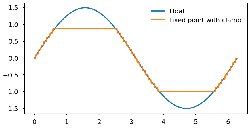
  • Decrease the number of integer bits, which reduces the range of the encoding. This can lead to misrepresent the signal using a particular encoding. For example, a sine with range [0, 8] can’t be encoded with U[4, 3] since numbers greater than \(2^{4} \cdot 2^{-3} = 2\) can’t be represented. This can have two different consequences over the signal:
    • Wrap: the signal is wrapped and the higher numbers are represented near the low values of the range.

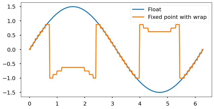
Example: S[4,3], range [-1, 0.875], resolution \(2^{-3} = 0.125\). If this encoding represent a number out of the range, \(1.125 = (01.001)_2 \), we only have 1 bit to represent the integer part. Therefore, it will be cut to \((1.001)_2\) which converting this 2’s complement number to decimal it is \( \left(-2^{3} + 2^{0} \right) \cdot 2^{-3} = -0.875\)

    • Clamp: all numbers outside the range are «saturated» to the maximum (or minimum) value. In order to represent the campling, it is necessary to include extra logic to take these cases into account.

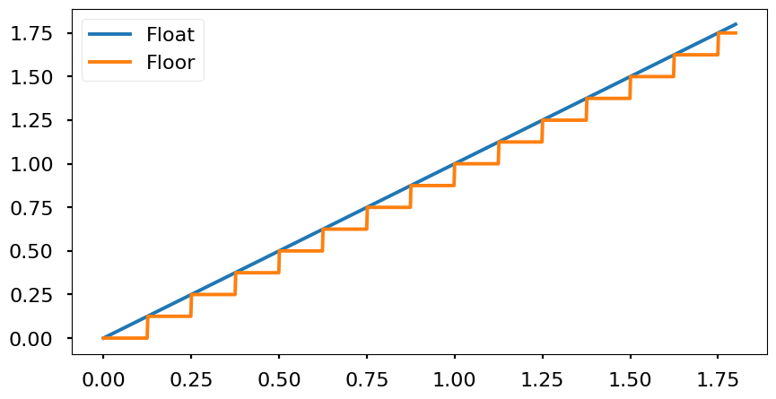
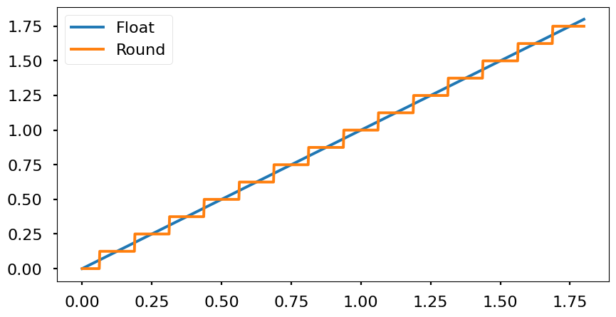
  • Quantization: since all decimal numbers can’t be represented due to the finite accuracy of the encoding, all possible values will be multiples of the resolution. Every real number between two multiples of the resolution will be mapped to one of the nearest multiples. Therefore, the signal will look like a stair wave. Depending the mapping technique used (nearest, floor, ceil, etc.) the effects are different. From the frequency point of view, the quantization adds white noise that is spreaded througout all the signal band (from 0 Hz to half of the sampling frequency \(\frac{f_s}{2}\).
    • Floor: «flooring» means to round to the nearest low value. This produces a maximum error of -Q and in average -Q/2. However, computationally is simple to resolve.

    • Nearest: round to the nearest value. It rounds up if Q/2 is exceeded and down if the value is below Q/2.

Implementation of nearest and floor

In MATLAB the functions round() and floor() can be used for computing the nearest and floor integer value of a number. Therefore, if we want to round to 2 decimals the number 12.5432 what we need to do is:

  • Shift two digits to the left multiplying the number by 100: 12.5432 · 100 = 1254.32
  • Apply the rounding method: floor(1254.32) = 1254
  • Shift two digits to the right dividing the number by 100: 1254/100 = 12.54

In the binary encoding, the operation is the same. The only difference is that instead of using powers of 10 to shift number, we use powers of 2.

Example: round to 3 fractional bits \(1.28515625 = (01.01001001)_2 \)

  • Shift 3 digits to the left multiplying by \(2^3\): \(1.28515625 \cdot 2^3 = 10.28125\)
  • Apply the floor() function. floor(10.28125) = 10
  • Shift 3 digits to the right multiplying by \(2^{-3}\): \(10 \cdot 2^{-3} = 1.25 = (01.010)_2\)

Quantizing fixed point number in MATLAB

In MATLAB we can use the function quatize(q, a). It can be used to compute the quantized number with a given fixed point encoding. This function has two parameters:

  • q: is the quantizer object that defines the enconding to be used. It is defined with the function quantizer(Format, Mode, Roundmode, Overflowmode), where:
    • Format: [N b]
    • Mode: ‘fixed’ o ‘ufixed’ for a fixed point encoding signed or unsigned.
    • Roundmode: ‘floor’, ‘round’ for nearest.
    • Overflowmode: ‘saturate’ or ‘wrap’
  • a: number to quantify

Definition of fixed point in Simulink

In Simulink, we can use the function fixdt(Signed, WordLength, FractionLength) to the define the encoding format.

Modifying the resolution or scaling

Extending the resolution

This is the situation in which we want to represent the fractional part with more bits than in the original encoding. This operation is as straightforward padding with zeros at the right of the binary number.

Reducing the resolution

The fractional part of the number is represented with less bits than in the original encoding. Therefore, the resolution is shrinked.

Example:

\(A = 2.625 = (010.101)_2\)

\(A [6,3] \rightarrow A =  A_e \cdot 2^{-3} =(010101)_2 ~~A_e = (010101)_2 21 \)

\(A’ [4,1] \rightarrow A’ =  A’_e \cdot 2^{-2} =(0101)_2~~A’_e = (0101)_2 = 5 \)

This operation can be intuitively understood as changing the integer part of the number. For instance, the initial number could be interpreted as unsigned as \(A_e = 21\) because the integer part was using 6 bits in total. If we cut the total number of bits used to 4, then the unsigned value is lower than before (5). FInally, if we need to scale the number moving the «fixed point» where necessary to obtain the final value on the new encoding.

Example:

\(A’_e = floor\left(A_e \cdot 2^{-2}\right) = 5\)

In this case, we need to multiply by \(2^{-2}\) because we need to go from a resolution of \(2^{-3}\) to \(2^{-1}\). Therefore, we need to shift the point 2 positions to the right.

The following circuit is known as a Schmitt trigger, implemented with BJT transistors. The main purpose of a Schmitt trigger is to generate a digital signal, which stated in other words is a signal whose only possible values are \(V_{cc}\) (logic 1) or ground (logic 0). The original analog signal can vary slowly in time so that the transition periods from high/low to low/high might not be fast enough. This circuit will act as a comparator with hysteresis whose thresholds for setting the output high or low will be defined by the design parameters.

Throughout the analysis we are going to consider for simplicity a voltage \(V_{be} = 0.6~V\) for the NPN to leave cut off and \(V_{ce} = 0.0~V\) when in saturation.

Since \(v_{in} = 5V\), \(Q_1\) is in saturation and in turn \(Q_2\) is cut off, then: \[i_2 = \frac{5~V}{1~k\Omega + 20~\Omega} = 4.9~mA\] \[i_3 = 0~mA\]\[v_{out} = 5~V\]\[v_{e} = i_2 \cdot R_4 = 4.9~mA · 20~\Omega = 98~mV\] \[v_{b1} = v_e + v_{be1} = 98~mV + 0.6~V \approx 0.7~V\]

A couple of details that can be extracted from here:

  • By having a voltage able to take \(Q_1\) into saturation, the output goes to \(V_{cc}\).
  • In order to get \(Q_1\) cut off, we need to drop \(in\) approximately \(100~mV\) higher than the \(v_{be}\) voltage, i.e., \(Q_1\) would cut off around \(in \approx 0.7~V\).

Therefore, let’s see what happens when from \(in = 5~V\) we drop \(in\) to \(0.7~V\).

\(Q_1\) and \(Q_2\) were in saturation and cut off respectively.
However, now that \(in = 0.7~V\), \(Q_1\) starts to stop driving current.
This makes the voltage at \(V_{b2}\) to rise due to a lower voltage drop across \(R_2\) and \(Q_2\) enters in saturation.
Since \(Q_2\) is in saturation, \(v_{be} = 0.6~V\)

In order to compute the currents going through the circuit in this state we can perform a mesh analysis taking into account the \(V_{BE}\) voltage between the base and the emitter and considering \(V_{CE} = 0\).

The two equations from meshes A and B are:
\[-V_{cc} + \left(R_2 + R_4\right)\cdot i_A + V_{be} – R_2\cdot i_B = 0\] \[-V_{be} – R_2\cdot i_A + \left(R_2 + R_3\right)\cdot i_B = 0\] Which can be written in matrix form as:\[\begin{pmatrix}
R_2 + R_4 & -R_2 \\
-R_2 & R_2 + R_3 \\
\end{pmatrix}
\begin{pmatrix}
i_A\\
i_B\\
\end{pmatrix} =
\begin{pmatrix}
V_{cc} – V_{be} \\
V_{be}
\end{pmatrix}\] Solving this equation as \(X = A^{-1} B\) we get that:\[i_A = 9.03~mA,~~ i_B = 4.81~mA\]With these current values, the voltage at the Q2 emitter is: \[V_{e} = i_A \cdot R_4 = 9.03~mA \cdot 20~\Omega = 180.6~mV\]

Again, what we can extract from these results is:

  • By having a voltage able to set \(Q_1\) cut off, the output goes to \(180~mV\), which in most of the digital families such as TTL or CMOS can be safely considered as a logic 0.
  • In order to get \(Q_1\) in saturation again, we need to increase \(in\) approximately \(180~mV\) above the \(v_{be} = 0.6\) voltage, i.e., \(Q_1\) would saturate around \(in \approx 0.78~V\).

So as we can see the circuit has hysteresis since thresholds for low to high and high to low are placed at different input voltages. This effect avoids having potentially multiple toggles at the output when the input voltage is near the threshold if the threshold would have been the same in both cases (low to high and high to low). Finally, the hysteresis voltage \(\Delta V\) can be approximated as \(\Delta V = \frac{R4}{R3} \cdot V_{cc}\).

LaTeX used to generate this article’s images:

\begin{circuitikz}
	\ctikzset{transistors/arrow pos=end}
	\draw (0,0) node[npn] (Q1){Q1};
	\draw (Q1.B) to[R, l2=$R_1$ and \SI{25}{\kilo\ohm}, l2 halign=c] ++(-1.5, 0) coordinate(in);
	\draw (in) to[short, -*] ++(-0.25,0) node[left]{in};
	\draw (Q1.C) -- +(1,0) node[npn, anchor=B](Q2){Q2} ;
	\draw (Q2.E) -- (Q2.E |- Q1.E);
	\draw (Q1.E) -- (Q1.E -| Q2.E);
	\draw (Q2.C) to[short, -*] +(0.5, 0) node[right]{out};
	\draw (Q1.E -| Q2.E) -- +(0, -0.25) to[R, l2=$R_4$ and \SI{20}{\ohm}] ++(0, -1.5) node[ground]{};
	\draw (Q1.C) -- (Q1.C |- Q2.C);
	\draw (Q1.C |- Q2.C)  to[R, l2=$R_2$ and \SI{1}{\kilo\ohm}, -*] ++(0, 2) coordinate(R2_top);
	\draw (Q2.C) to[R, l2_=$R_3$ and \SI{1}{\kilo\ohm}, -*] ++(0, 2) coordinate (R3_top);
	\draw (R3_top) -- (R2_top) -- +(-0.5, 0);
	\draw (R3_top) -- +(0.5, 0)  node[right]{$V_{cc}$};
\end{circuitikz}
\begin{circuitikz}
        \ctikzset{transistors/arrow pos=end}
	\draw (0,0) node[npn] (Q1){Q1};
	\draw (Q1.B) to[R, l2=$R_1$ and \SI{10}{\kilo\ohm}, l2 halign=c, f<_=\SI{430}{\micro\ampere}, current arrow scale=24] ++(-1.5, 0) coordinate(in);
	\draw (Q1.B) node[below, xshift=-2]{$+$};
    \draw (Q1.E) node[anchor=south east, yshift=-9]{$-$};
    %\draw ($(Q1.B)!0.5!(Q1.E)$) coordinate(vbe_label);
    %\draw (vbe_label) node[yshift=-3, xshift=-2]{$V_{be1}$};
    \draw (Q1) node[anchor=north east, yshift=-7, xshift=-3]{$V_{be1}$};
	\draw (in) to[short, -*] ++(-0.25,0) node[left]{$\text{in} = \SI{5}{\volt}$};
	\draw (Q1.C) -- +(1,0) node[npn, anchor=B](Q2){Q2} ;
	\draw (Q2.E) -- (Q2.E |- Q1.E);
	\draw (Q1.E) -- (Q1.E -| Q2.E);
	\draw (Q2.C) to[short, -*] +(0.5, 0) node[right]{out};
	\draw (Q2.B) node[below, xshift=-3]{$+$};
    \draw (Q2.E) node[left, yshift=-3]{$-$};
	\draw (Q2) node[anchor=north east, yshift=-9, xshift=-5]{$V_{be2}$};
	\draw (Q1.E -| Q2.E) -- +(0, -0.25) coordinate(R4_top) to[R, l2=$R_4$ and \SI{20}{\ohm}, f_=\SI{5.43}{\milli\ampere}, l2 halign=c] ++(0, -1.5) node[ground]{};
	\draw (Q1.C) -- (Q1.C |- Q2.C);
	\draw (Q1.C |- Q2.C)  to[R, l2=$R_2$ and \SI{1}{\kilo\ohm}, -*, f<^=\SI{4.9}{\milli\ampere}, l2 halign=c] ++(0, 2) coordinate(R2_top);
	\draw (Q2.C) to[R, l2_=$R_3$ and \SI{1}{\kilo\ohm}, -*, f<^=\SI{0}{\milli\ampere}, l2 halign=c] ++(0, 2) coordinate (R3_top);
	\draw (R3_top) -- (R2_top) -- +(-0.5, 0);
	\draw (R3_top) -- +(0.5, 0)  node[right]{$V_{cc}=\SI{5}{\volt}$};
\end{circuitikz}
\begin{circuitikz}
	\draw (0, 0) to[R, l2_=$R_2$ and \SI{1}{\kilo\ohm}] +(0, -2) coordinate(R2_bottom);
	\draw (R2_bottom) to[vsource, l_=$V_{BE}$]  +(2, 0) coordinate(QB);
	\draw (R2_bottom -| QB) to[R, l2_=$R_3$ and \SI{1}{\kilo\ohm}] +(0, 2) coordinate(R3_top);
	\draw (QB) to [R, l=$R_4$, l2=$R_4$ and \SI{20}{\ohm}] +(0, -2) coordinate (R4_bottom);
	\draw (0,0) -- (R3_top);
	\draw (0,0) -- (-2.5, 0) -- (-2.5, -1.75);
	\draw (-2.5, -1.75) to[vsource, l=$V_{CC}$] +(0, -1.0) coordinate(Vcc_bottom) -- (R4_bottom -| Vcc_bottom) -- (R4_bottom);
	 \draw [Latex-]  (1.0,-1.25) coordinate(loop) node [anchor=center, yshift=10] {$i_B$} arc (-90:145:3.5mm);
	 \draw [Latex-]  (-0.75,-3.25) coordinate(loop) node [anchor=center, yshift=13] {$i_A$} arc (-90:145:4.5mm);
\end{circuitikz}

The LaTeX package CircuiTikZ is an excelent way to draw circuits in a standard and elegant manner. However, it can get quite tricky when you need to specify the absolute coordinates of all the nodes of your schematic.

In order to facilitate this process coordinates and orthogonal coordinates come to the rescue.

Coordinates

You can provide a name for every node in your circuit. For instance, in the following line:

\draw (0,0) -- (2,0) coordinate(pointA);

point (2,0) can be accessed from now on using (pointA):

\draw (0,0) -- (2,0) coordinate(pointA);
\draw (pointA) to[R] ++(2,0);

The resistor will be placed from pointA, i.e., (2,0), to (4,0). Remember that the operator ++() makes a relative movement with respect the previous point (in this case (2,0)) and «stores» the position so that any new component in the same \draw statement will start from that point, i.e., (4,0). Also, +() makes the relative movement with respect the original point without storing the new position and not affecting any subsequent element in the \draw statement.

When using hardcoded coordinates like in previous example it might not be very powerful per se, but at least it may help to understand the way the diagram is written.

However, they can solve a lot of headaches when you need to draw two or more components in parallel.

Orthogonal coordinates

In case you want to align to different nodes, orthogonal coordinates computes automatically the X and Y of the new node.

From CircuiTikZ manual, section 2.2, where a classic non-inverting amplifier using an op amp is being drawn:

\draw (FB) to[R=$R_2$] (FB -| OA.out) -- (OA.out)

The way the previous line can be read is:

  1. From the coordinate FB, add a resistor to
  2. The horizontal value of FB (that’s why - is next to FB) and the veritical of OA.out (that’s why | is before OA.out)
  3. Then draw a line from this previous point to the op amp output OA.out

Example

Below you will find an example where all previous concepts are applied in order to draw the schematic of a basic pulse generator with BJT’s.

\usepackage[american]{circuitikz}
\usepackage{siunitx}

\begin{circuitikz} []
   \draw (0,0) node[bjtnpn] (Q1){Q1};
   \draw (Q1.B) to[R, l2={$R_1$ and \SI{10}{\kilo\ohm}}, l2 halign =c] ++(-2,0) to[short,-o] ++(-0.1, 0) node[above]{in};
   \draw (Q1.C) to[R, l2={$R_2$ and \SI{1}{\kilo\ohm}}] ++(0, 2) coordinate(R2t);
   \draw (Q1.E) to[short] ++(0, -0.1) coordinate(Q1gnd) node[ground] (GND){} ;
   \draw (Q1.C) to[C, l2_=$C_1$ and \SI{10}{\nano\farad}, l2 halign =c] ++(2.5,0) coordinate(c1n) to[short] +(0,-1) node[bjtnpn, anchor=B](Q2){Q2};
   \draw (c1n) to[R,l2=$R_3$ and \SI{10}{\kilo\ohm}] ++(0,2) coordinate (R3t);
   \draw (R2t) -- (R3t);
   \draw (R2t) -- +(-0.5,0);
   \draw (R3t) -- +(0.5, 0);
   \draw (Q2.E) -- (Q2.E |- Q1gnd) node[ground]{};
   \draw (Q2.C) -- (Q2.C |- c1n) coordinate(R4b) to[R,l2_=$R_4$ and \SI{1}{\kilo\ohm}] (Q2.C |- R2t) coordinate(R4t) -- (R3t);
   \draw (R4t) -- ++(0.5,0);
   \draw (Q2.C) to[short, -o] ++(1,0) node[above]{out};
\end{circuitikz}

Design a full-wave bridge rectifier circuit to deliver 10 V dc with less than 0.1 V (pp) ripple into a load drawing up to 10 mA. Choose the appropriate ac input voltage, assuming 0.6 V diode drops. Be sure to use the correct ripple frequency in your calculation.

The relationship between current and voltage in a capacitor is:
\[ Q = C \cdot V \]\[ \int{I dt} = C \cdot V \]\[ I dt = C \cdot dV \Rightarrow I = C \frac{dV}{dt} \]\[ dV = \frac{I}{C} dt \]\[ \Delta V = \frac{I}{C} \Delta t~~~\left(1\right) \]

Frequency of the ac signal: \(f\)
\(\Delta t = \frac{1}{2f}\)

If we need \(\delta V = 0.1~Vpp\) by drawing 10 mA, then, from Equation 1:
\[ \Delta V = \frac{I}{C} \Delta t \]\[ C = \frac{I}{\Delta V} \Delta t\]\[ C = \frac{10^{-2}}{0.1~V}\cdot \frac{1}{2f}\]

Let’s assume \(f = 60 Hz\), then:
\[C = \frac{10^{-2}~A}{0.1~V}\cdot \frac{1}{2\cdot 60~Hz} = 833~\mu F\]

The capacitor is going to be charged to the input amplitude – the diode voltage drop. Therefore, the amplitude of the ac input voltage should be:
\[ V_{out~max~pp} = V_{in~pp} – 2 \cdot V_{diode~drop}\]\[
V_{in~pp} = V_{out~max~pp} + 2 \cdot V_{diode~drop} = 10~V + 2\cdot 0.6~V = 11.2~V
\]
If simulated on a SPICE simulator, the results are confirmed. The difference on the final rectified voltage comes from the dynamic behaviour of the model used for the diodes, which is not an ideal model with 0.6 V threshold as assumed in the exercise’s data. The approximation of 0.6 V drop is more or less decent since the final voltage is around 9.5 V.

Therefore, the key aspects to remember from this circuit are:

  1. The output voltage only depends on the input voltage
  2. The ripple depends both in the output current and the capacitance value. The more current, the more charge is extracted from the capacitor. Therefore, voltage discharge increases. Same rationale works on the capacitance: the greater the capacitance, the more charge can be stored for a given capacitor voltage

Basic operation

The left hand side of the keyboard uses a Microchip MCP23018 IC, which is an I/O expander with open drain outputs and it can be configured through I2C or SPI. In this case we are going to focus on the I2C protocol only since it is the one used by the main MCU. The MCU is a Teensy 2.0 and it is placed on the right hand side of the Ergodox. It is used for monitoring all the switch status, converting the pressed switches into its corresponding character and sending it through USB to interact with the computer as a usual keyboard.

The MCP23018 has two different GPIO ports, GPIOA and GPIOB, each with 8 I/O pads. In the original Ergodox PCB, port A is used to interact with the columns and port B with the rows.
GPIO pads on port B (rows) are configured as inputs and the internal pull-up resistor is enabled on every port B pad. Regarding GPIO pads on port A, they are configured as outputs. According to the datasheet, output pads on the MCP23018 are open-drain, which basically means that the pad value can be internally driven to ground or left floating (high impedance). Since the rows and columns are connected through the mechanical switch and the diode, GPIO’s on port B can determine if the switch is closed (pressed) or open (released) depending on the voltage found at it. A diagram of this scheme is shown below.

The way the Ergodox firmware determines the state of every switch (closed/pressed or open/released) is by sequentially setting one column to ground while leaving the rest floating. Then, the state of the rows is read. Depending on the state of the switch, the GPIOB reading will be:

  • If the switch is released, the voltage at GPIOB will be VDD due to its pull-up resistor. The pad value will be read as 1.
  • If the switch is closed, the voltage at GPIOB will be set to 0.0 V. The pad value will be read as 0.

Since the rest of columns are left floating, they won’t interfere on the reading. Once the state of a particular row is read, its value is stored and the operation is repeated until all the available rows are covered. The process of reading the state of all the switches is called a «scan».

Debugging MCP23018 with Arduino

When I assembled my Ergodox, I loaded the QMK firmware expecting the keyboard to just work. However, there seems to be a hardware issue since the comunication between the LHS and the RHS is not successful. Therefore, I decided to replicated the QMK firmware on an Arduino to have a better understanding on how the MCP and the Teensy interact together and also figure out if there’s really any hardware issue on the PCB’s.

QMK firmware is highly customizable and therefore it can be a little bit intricate when trying to read its code. I tried to distil the most basic functionality regarding the writing and reading done from the Teensy to the Mcp23018 through I2C.

The code below will perform a scan every 1 second and will print through the Serial interface the keyboard matrix result.

mcp23018_debug.c

#include <Wire.h>
#include "mcp23018.h"
#include "i2c_wrapper.h"
#include "utils.h"

#define KB_ROWS     6
#define KB_COLUMNS  7  // 14 in total, 7 in left hand side

int data;
bool matrix[KB_ROWS][KB_COLUMNS];

void setup() {
  Wire.begin();

  Serial.begin(9600);
  while (!Serial); // Leonardo: wait for Serial Monitor
  Serial.println("\nMCP23018 debugger");
  delay(2000);

  mcp23018_init();
}

void loop() {

  while(true) {
    // Clear matrix values
    clear_matrix();

    for (uint8_t col = 0; col < KB_COLUMNS; col++) {
      // Drive column to ground
      drive_column(col);
      // Read GPIO's on port B
      data = i2c_rd(I2C_ADDR, GPIOB);
      for (uint8_t row=0; row < KB_ROWS; row++) {
        // Store read values into the matrix
        matrix[row][col] = !( data & (1<<(5-row)) );
      }
    }

    print_matrix();
    // Leave column floating again
    drive_column_hiz();
    // Wait 1 second
    delay(1000);
  }

}

void drive_column(uint8_t col) {
   i2c_wr(I2C_ADDR, GPIOA, 0xFF & ~(1 << col));
}

void drive_column_hiz() {
  i2c_wr(I2C_ADDR, GPIOA, 0xFF);
}

void clear_matrix() {
  for (uint8_t row = 0; row < KB_ROWS; row++) {
    for (uint8_t col = 0; col < KB_COLUMNS; col++) {
       matrix[row][col] = 0;
    }
  }
}

void print_matrix() {
   for (uint8_t col = 0; col < KB_COLUMNS; col++) {
      if (col == 0) {
        Serial.println("[ ");
      }
      for (uint8_t row = 0; row < KB_ROWS; row++) {
         Serial.print(matrix[row][col] ? 1 : 0);
         Serial.print("  ");
      }
      Serial.println();
      if (col == 6) {
        Serial.println("]");
      }
   }
}

Output:

MCP23018 debugger
[ 
0  0  0  0  0  0  
0  0  0  0  1  0  
0  0  0  0  0  0  
0  0  0  0  0  0  
0  0  0  0  0  0  
0  0  0  0  0  0  
0  0  0  0  0  0  
]

where 1 means the switch is pressed and 0 released.

Auxiliary files

i2c_wrapper.h

#include <Wire.h>

int i2c_rd(int i2c_addr, int reg_addr) {
   int rd_data;
   // Start condition + 7 bit I2C device address
   Wire.beginTransmission(i2c_addr);
   // Write bit + next byte
   Wire.write(reg_addr);
   // Stop condition
   Wire.endTransmission();
   // Start condition + address + read bit
   Wire.requestFrom(i2c_addr, 1); // request 1 byte from slave device
   if(Wire.available()) {
    rd_data = Wire.read();
   }
   Wire.endTransmission();
   return rd_data;
}

int i2c_wr(int i2c_addr, int reg_addr, uint8_t wr_data) {
   // Start condition + 7 bit I2C device address
   Wire.beginTransmission(I2C_ADDR);
   // Byte with address to be written
   Wire.write(reg_addr);
   // Data to be written
   Wire.write(wr_data);
   // Stop condition
   return Wire.endTransmission();
}

mcp23018.h

#define I2C_ADDR        0b0100000
// i/o direction register
#define IODIRA          0x00
#define IODIRB          0x01
// GPIO pull-up resistor register
#define GPPUA           0x0C
#define GPPUB           0x0D
// general purpose i/o port register (write modifies OLAT)
#define GPIOA           0x12
#define GPIOB           0x13

utils.h

#ifndef _UINT8_T
#define _UINT8_T
typedef unsigned char uint8_t;
#endif /* _UINT8_T */

int print_addr_val(int addr, int val) {
    Serial.print("Addr ");
    Serial.print(addr, HEX);
    Serial.print(": ");
    Serial.println(val, BIN);
}